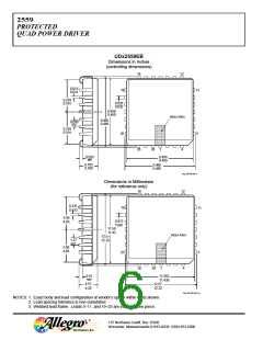
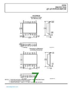
2559
PROTECTED
QUAD POWER DRIVER
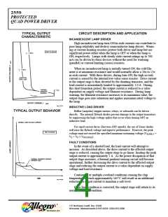
TYPICAL OUTPUT
CHARACTERISTIC
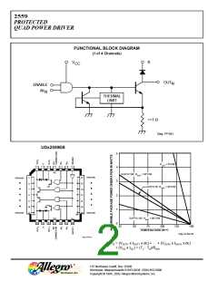
CIRCUIT DESCRIPTION AND APPLICATION
INCANDESCENT LAMP DRIVER
High incandescent lamp turn-ON/in-rush currents can contribute to
poor lamp reliability and destroy semiconductor lamp drivers. Warm-
ing or current-limiting resistors protect both driver and lamp but use
significant power either when the lamp is OFF or when the lamp is
ON, respectively. Lamps with steady-state current ratings up to 700
mA can be driven by these devices without the need for warming
(parallel) or current-limiting (series) resistors.
NOT TO SCALE
T
< 150°C
J
When an incandescent lamp is initially turned ON, the cold fila-
ment is at minimum resistance and would normally allow a 10x to 12x
in-rush current. With these drivers, during turn-ON, the high in-rush
current is sensed by the internal low-value sense resistor. Drive current
to the output stage is then diverted by the shunting transistor, and the
load current is momentarily limited to approximately 1.0 A. During
this short transition period, the output current is reduced to a value
dependent on supply voltage and filament resistance. During lamp
warmup, the filament resistance increases to its maximum value, the
output stage goes into saturation and applies maximum rated voltage to
the lamp.
T
= 165°C
J
JUNCTION
TEMP. LIMIT
THERMAL
GRADIENT
SENSING
I TRIP
V
OUT(SAT)
OUTPUT CURRENT, I
OUT
Dwg. GP-013
INDUCTIVE LOAD DRIVER
TYPICAL OUTPUT BEHAVIOR
Bifilar (unipolar) stepper motors, relays, or solenoids can be driven
directly. The internal flyback diodes prevent damage to the output transistors
by suppressing the high-voltage spikes that occur when turning OFF an
inductive load.
NORMAL LAMP IN-RUSH CURRENT
For rapid current decay (fast turn-OFF speeds), the use of Zener diodes
will raise the flyback voltage and inprove performance. However, the peak
NOT TO SCALE
voltage must not exceed the specified minimum sustaining voltage (VSUPPLY
+
VZ + VF ≤ VOUT(SUS)).
FAULT CONDITIONS
In the event of a shorted load, the load current will attempt to
increase. As described above, the drive current to the affected output
stage is reduced, causing the output stage to go linear, limiting the peak
output current to approximately 1 A. As the power dissipation of that
output stage increases, a thermal gradient sensing circuit will become
operational, further decreasing the drive current to the affected output
stage and reducing the output current to a value dependent on supply
voltage and load resistance.
THERMAL GRADIENT SENSING
CURRENT LIMIT
ITRIP
Continuous or multiple overload conditions causing the chip
temperature to reach approximately 165°C will result in an additional
reduction in output current to maintain a safe level.
0
TIME
Dwg. WP-008
If the fault condition is corrected, the output stage will return to its
normal saturated condition.
115 Northeast Cutoff, Box 15036
Worcester, Massachusetts 01615-0036 (508) 853-5000

 ALLEGRO [ ALLEGRO MICROSYSTEMS ]