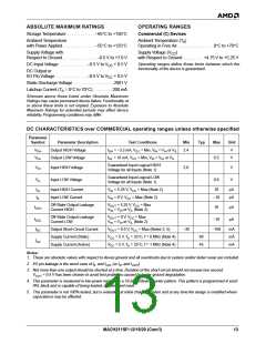
ABSOLUTE MAXIMUM RATINGS
OPERATING RANGES
Storage Temperature . . . . . . . . . . . . –65°C to +150°C
Commercial (C) Devices
Ambient Temperature
Ambient Temperature (T )
A
with Power Applied. . . . . . . . . . . . . . –55°C to +125°C
Operating in Free Air. . . . . . . . . . . . . . . .0°C to +70°C
Supply Voltage with
Supply Voltage (V
)
CC
Respect to Ground. . . . . . . . . . . . . . . –0.5 V to +7.0 V
with Respect to Ground . . . . . . . . +4.75 V to +5.25 V
Operating ranges define those limits between which the
functionality of the device is guaranteed.
DC Input Voltage . . . . . . . . . . . .–0.5 V to V + 0.5 V
CC
DC Output or
I/O Pin Voltage . . . . . . . . . . . . . .–0.5 V to V + 0.5 V
CC
Static Discharge Voltage . . . . . . . . . . . . . . . . . 2001 V
Latchup Current (T = 0°C to 70°C). . . . . . . . 200 mA
A
Stresses above those listed under Absolute Maximum
Ratings may cause permanent device failure. Functionality at
or above these limits is not implied. Exposure to Absolute
Maximum Ratings for extended periods may affect device
reliability. Programming conditions may differ.
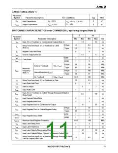
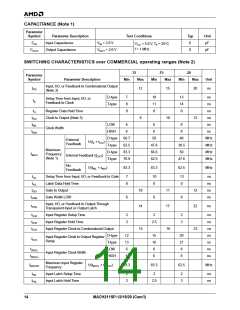
DC CHARACTERISTICS over COMMERCIAL operating ranges unless otherwise specified
Parameter
Symbol
Parameter Description
Output HIGH Voltage
Test Conditions
= –3.2 mA, V = Min, V = V or V
IL
Min
Typ
Max
Unit
V
V
I
2.4
OH
OH
CC
IN
IH
V
Output LOW Voltage
I
= 16 mA, V = Min, V = V or V
IL
0.5
V
OL
OL
CC
IN
IH
Guaranteed Input Logical HIGH
Voltage for all Inputs (Note 1)
V
Input HIGH Voltage
Input LOW Voltage
2.0
V
V
IH
Guaranteed Input Logical LOW
Voltage for all Inputs (Note 1)
V
0.8
IL
I
Input HIGH Current
Input LOW Current
V
= 5.25 V, V = Max (Note 2)
10
µA
µA
IH
IN
CC
I
V
= 0 V, V = Max (Note 2)
–10
IL
IN
CC
Off-State Output Leakage
Current HIGH
V
= 5.25 V, V = Max
= V or V (Note 2)
IH IL
OUT CC
I
10
µA
µA
OZH
V
IN
Off-State Output Leakage
Current LOW
V
= 0 V, V = Max
= V or V (Note 2)
IH IL
OUT CC
I
–10
OZL
V
IN
I
Output Short-Circuit Current
Supply Current (Static)
Supply Current (Active)
V
= 0.5 V, V = Max (Notes 3, 5)
–30
–160
mA
mA
mA
SC
OUT
CC
V
= 5 V, T = 25°C, f = 0 MHz (Note 4)
40
45
CC
A
I
CC
V
= 5 V, T = 25°C, f = 1 MHz (Note 4)
A
CC
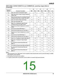
Notes:
1. These are absolute values with respect to device ground and all overshoots due to system and/or tester noise are included.
2. I/O pin leakage is the worst case of I and I (or I and I ).
IL
OZL
IH
OZH
3. Not more than one output should be shorted at a time. Duration of the short-circuit should not exceed one second.
= 0.5 V has been chosen to avoid test problems caused by tester ground degradation.
V
OUT
4. This parameter is measured in low-power mode with a 16-bit up/down counter pattern. This pattern is programmed in each
PAL block and is capable of being loaded, enabled and reset.
5. This parameter is not 100% tested, but is evaluated at initial characterization and at any time the design is modified where
capacitance may be affected.
MACH211SP-12/15/20 (Com’l)
13

 AMD [ AMD ]