AUSTIN SEMICONDUCTOR, INC.
FLASH
AS8FLC2M32
Austin Semiconductor, Inc.
When the Embedded Erase Algorithm is complete, the device
returns to READING Array data and addresses are no longer
latched. The system can determine the status of the ERASE
operation by using DQ2, DQ6, and DQ7 of Byte 1; DQ10, DQ14
and DQ15 of Byte 2; DQ18, DQ22 and DQ23 of Byte 3 as well as
DQ26, DQ30 and DQ31 of Byte 4. In addition to the Data IO
indicators, the system/user my monitor RY/BY\ for the status
of the operation.
Any commands WRITTEN to the chip during the Embedded
ERASE operation are ignored. Note that a HARDWARE RESET
during the chip erase operation immediately terminates the
operation. The CHIP ERASE command sequence should be
reinitiated once the device has returned to READING Array
data, to ensure data integrity.
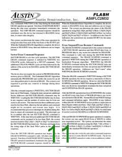
The system can determine the status of the erase operation by
using byte data from each of the four bytes or the RY/BY\ pin.
When the Embedded ERASEAlgorithm is complete, the device
returns to READING Array data and Addresses are no longer
latched.
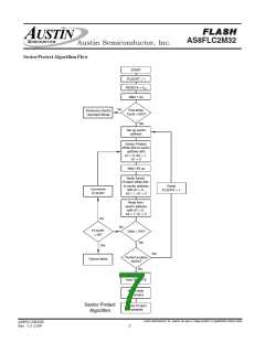
Erase Suspend/Erase Resume Commands
The ERASE SUSPEND command allows the system to interrupt
a SECTOR ERASE operation and then READ data from, or
PROGRAM data to, any sector not selected for ERASURE.
This command is valid only during the SECTOR ERASE
command sequence. The ERASE SUSPEND command is
ignored if WRITTEN during the CHIP ERASE operation or
Embedded Program algorithm. WRITING the ERASE
SUSPEND command during the SECTOR ERASE time-out
immediately terminates the time-out period and SUSPENDS
the ERASE operation. Addresses are “don’t-cares” when
WRITING the ERASE SUSPEND command.
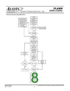
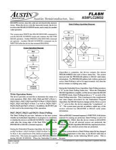
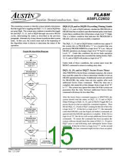
Sector Erase Command Sequence
SECTOR ERASE is a six-bus cycle operation. The SECTOR
ERASE command sequence is initiated by WRITING two
UNLOCK cycles, followed by a SET-UP command. Two
additional UNLOCK WRITE cycles are then followed by the
address of the sector to be ERASED, and the SECTOR ERASE
command.
The device does not require the system to PREPROGRAM the
memory prior to ERASE. The Embedded ERASE Algorithm
automatically PROGRAMS and verifies the sector for an all
zero data pattern prior to electrical ERASE. The system is not
required to provide any controls or timings during these
operations.
When the ERASE command is WRITTEN during a SECTOR
ERASE operation, the device requires a maximum of 20us to
SUSPEND the ERASE operation. However, when the ERASE
SUSPEND command is WRITTEN during the SECTOR ERASE
time-out, the device immediately terminates the time-out period
and SUSPENDS the ERASE operation.
After the command sequence is WRITTEN, a SECTOR ERASE
time-out of 50uS begins. During the time-out period, additional
Sector Addresses and SECTOR ERASE commands may be
WRITTEN. Loading the SECTOR ERASE buffer may be done
in any sequence and the number of sectors may be from one
sector to all sectors. The time between these additional cycles
must be less than 50uS, otherwise the last address and command
might not be accepted, and erasure may begin. It is
recommended that processor interrupts be disabled during this
time to ensure all commands are accepted. The interrupts can
be re-enabled after the last SECTOR ERASE command is
WRITTEN. If the time between additional SECTOR ERASE
commands can be assumed to be less than 50uS, the system
need not monitor DQ3, DQ11, DQ19 or DQ27 to determine if
the SECTOR ERASE has timed out. The time-out begins from
the rising edge of the final WEx\ pulse in the command
sequence.
After the ERASE operation has been SUSPENDED, the system
can READ Array data from or PROGRAM data to any sector
not selected for ERASURE. Normal READ and WRITE timings
and command definitions apply. READING at any Address
within ERASE-SUSPENDED sectors produces status data on
three DQ pins within each Byte. DQ2, DQ6, and DQ7 of Byte 1;
DQ10, DQ14 and DQ15 of Byte 2; DQ18, DQ22 and DQ23 of
Byte 3 as well as DQ26, DQ30 and DQ31 of Byte 4 to determine
if a sector is actively ERASING or is ERASE-SUSPENDED.
After and ERASE-SUSPENDED program operation is complete,
the system can once again READ from or WRITE to within
non-suspended sectors. The system can determine the status
of the PROGRAM operation using the DQ6, 7 bits of Byte 1;
DQ14, 15 of Byte 2; DQ22, 23 of Byte 3 and DQ30, 31 of Byte 4;
just as in the standard PROGRAM operation.
The system may also write the auto select command sequence
when the device is in the ERASE SUSPEND mode. The device
allows READING autoselect codes even at addresses within
Once the SECTOR ERASE operation has begun, only the
ERASE SUSPEND command is valid. All other commands are
ignored. Note that a HARDWARE RESET during the SECTOR
ERASE operation immediately terminates the operation. The
SECTOR ERASE command sequence should be reinitiated
once
Austin Semiconductor, Inc. reserves the right to change products or specifications without notice.
AS8FLC2M32B
Rev. 1.2 5/09
11

 AUSTIN [ AUSTIN SEMICONDUCTOR ]