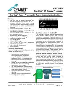
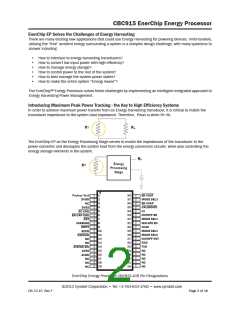
CBC915 EnerChip Energy Processor
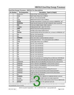
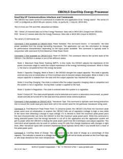
EnerChip Energy Processor CBC915 Operating and Maximum Parameters
Parameter
Recommended Operating Conditions
Supply voltage VDD
Min
Typ
Max
Unit
2.5
3.5
3.6
V
Supply voltage VSS
-
0
-
V
Operating temperature - CBC915-ACB
Operating temperature - CBC915-AIB
Absolute Maximum Ratings
Voltage applied at VDD to VSS
Voltage applied to any pin
-20
-40
+25
+25
+70
+85
°C
°C
-0.3
-0.3
-2
-
-
-
-
4.1
VDD+0.3
-2
V
V
Diode current at any device terminal
Storage temperature range
mA
°C
-55
+105
Notes:
1. Thermal or electrical stresses beyond those listed under absolute maximum ratings may cause permanent damage
to the CBC915. These are stress ratings only, and functional operation of the device at these or any other conditions
beyond those indicated under recommended operating conditions is not implied. Exposure to absolute maximum rated
conditions for extended periods my affect device reliability.
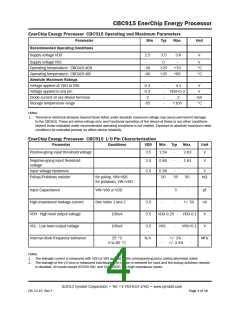
EnerChip Energy Processor CBC915 I/O Pin Characterization
Parameter
Conditions
VDD
Min
Typ
Max
Unit
Positive-going input threshold voltage
3.5
1.59
-
2.63
V
Negative-going input threshold
voltage
3.5
3.5
0.88
-
1.91
V
Input voltage hysteresis
Pullup/Pulldown resistor
0.36
20
-
-
V
for pullup, VIN=VSS
35
50
kΩ
for pulldown, VIN=VDD
Input Capacitance
VIN=VSS or VDD
See notes 1 and 2
100uA
-
-
5
-
-
pF
nA
V
High impedance leakage current
VOH - High level output voltage
VOL - Low level output voltage
Internal clock frequency tolerance
3.5
3.5
3.5
N/A
+/- 50
VDD-0.25 - VDD-0.1
100uA
VSS
-
VSS+0.1
-
V
25 °C
0 to 80 °C
-
-
+/- 1%
+/- 2.5%
MHz
-
Notes:
1. The leakage current is measured with VDD or VSS applied to the corresponding pin(s) unless otherwise noted.
2. The leakage of the I/O pins is measured individually. The I/O pin is selected for input and the pullup/pulldown resistor
is disabled. All inputs except STATUS SW/ and CALIBRATE/ are high impedance inputs.
©2012 Cymbet Corporation • Tel: +1-763-633-1780 • www.cymbet.com
DS-72-15 Rev F
Page 4 of 16

 CYMBET [ CYMBET CORPORATION ]