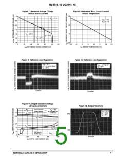
UC3844, 45 UC2844, 45
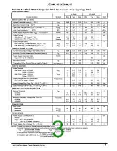
ELECTRICAL CHARACTERISTICS (V
unless otherwise noted,)
= 15 V, [Note 2], R = 10 k, C = 3.3 nF, T = T
to T
[Note 3],
high
CC
T
T
A
low
UC284X
Typ
UC384X
Characteristics
Symbol
Min
Max
Min
Typ
Max
Unit
ERROR AMPLIFIER SECTION
Voltage Feedback Input (V = 2.5 V)
V
I
2.45
–
2.5
–0.1
90
2.55
–1.0
–
2.42
–
2.5
–0.1
90
2.58
–2.0
–
V
µA
O
FB
Input Bias Current (V
= 2.7 V)
FB
Open Loop Voltage Gain (V = 2.0 V to 4.0 V)
IB
A
VOL
BW
65
0.7
60
65
0.7
60
dB
O
Unity Gain Bandwidth (T = 25°C)
1.0
70
–
1.0
70
–
MHz
dB
J
Power Supply Rejection Ratio (V
= 12 V to 25 V)
PSRR
–
–
CC
Output Current
mA
Sink (V = 1.1 V, V
Source (V = 5.0 V, V
O
= 2.7 V)
I
Sink
Source
2.0
–0.5
12
–1.0
–
–
2.0
–0.5
12
–1.0
–
–
O
FB
= 2.3 V)
I
FB
Output Voltage Swing
V
High State (R = 15 k to ground, V
= 2.3 V)
FB
= 2.7 V)
V
OH
V
OL
5.0
–
6.2
0.8
–
1.1
5.0
–
6.2
0.8
–
1.1
L
Low State (R = 15 k to V , V
L
ref FB
CURRENT SENSE SECTION
Current Sense Input Voltage Gain (Notes 4 & 5)
Maximum Current Sense Input Threshold (Note 4)
Power Supply Rejection Ratio
A
2.85
0.9
3.0
1.0
3.15
1.1
2.85
0.9
3.0
1.0
3.15
1.1
V/V
V
V
V
th
PSRR
dB
V
= 12 V to 25 V (Note 4)
–
–
–
70
–
–
–
–
70
–
CC
Input Bias Current
I
–2.0
150
–10
300
–2.0
150
–10
300
µA
IB
Propagation Delay (Current Sense Input to Output)
t
ns
PLH(IN/OUT)
OUTPUT SECTION
Output Voltage
V
Low State (I
= 20 mA)
= 200 mA)
= 20 mA)
= 200 mA)
V
–
–
12
12
0.1
1.6
13.5
13.4
0.4
2.2
–
–
–
13
12
0.1
1.6
13.5
13.4
0.4
2.2
–
Sink
Sink
Sink
Sink
OL
(I
High State (I
(I
V
OH
–
–
Output Voltage with UVLO Activated
= 6.0 V, I = 1.0 mA
V
OL(UVLO)
V
V
CC
–
–
–
0.1
50
50
1.1
150
150
–
–
–
0.1
50
50
1.1
150
150
Sink
Output Voltage Rise Time (C = 1.0 nF, T = 25°C)
t
r
ns
ns
L
J
Output Voltage Fall Time (C = 1.0 nF, T = 25°C)
t
f
L
J
UNDERVOLTAGE LOCKOUT SECTION
Startup Threshold
UCX844
UCX845
V
V
V
th
15
7.8
16
8.4
17
9.0
14.5
7.8
16
8.4
17.5
9.0
Minimum Operating Voltage After Turn–On
UCX844
UCX845
V
CC(min)
9.0
7.0
10
7.6
11
8.2
8.5
7.0
10
7.6
11.5
8.2
PWM SECTION
Duty Cycle
Maximum
Minimum
%
DC
46
–
48
–
50
0
47
–
48
–
50
0
max
DC
min
TOTAL DEVICE
Power Supply Current (Note 2)
Startup:
I
mA
V
CC
(V
(V
CC
= 6.5 V for UCX845A,
14 V for UCX844) Operating
–
–
0.5
12
1.0
17
–
–
0.5
12
1.0
17
CC
Power Supply Zener Voltage (I = 25 mA)
V
30
36
–
30
36
–
CC
Z
NOTES: 2. Adjust V
above the Startup threshold before setting to 15 V.
CC
3. Low duty cycle pulse techniques are used during test to maintain junction temperature as close to ambient as possible
T
T
= –20°C for UC3844, UC3845
= –25°C for UC2844, UC2845
T
T
= +70°C for UC3844, UC3845
= +85°C for UC2844, UC2845
= 0 V.
low
low
high
high
FB
4. This parameter is measured at the latch trip point with V
∆V Output Compensation
5. Comparator gain is defined as: A
V
∆V Current Sense Input
3
MOTOROLA ANALOG IC DEVICE DATA

 FREESCALE [ Freescale ]