Global Mixed-mode Technology Inc.
G1426
Absolute Maximum Ratings
Supply Voltage, VCC…………………..…...…….……...6V
Operating Ambient Temperature Range
Power Dissipation (1)
TA ≤ 25°C………………………………………….2.7W
TA ≤ 70°C………………………………………….1.7W
TA ≤ 85°C………………….………………………1.4W
Electrostatic Discharge, VESD
TA…….…………………………….……….-40°C to +85°C
Maximum Junction Temperature, TJ…..……….….150°C
Storage Temperature Range, TSTG….….-65°C to+150°C
Soldering Temperature, 10seconds, TS……….……260°C
Human body mode..…………………….-3000 to 3000(2)
Note:
(1) : Recommended PCB Layout
(2) : Human body model : C = 100pF, R = 1500Ω, 3 positive pulses plus 3 negative pulses
Electrical Characteristics
DC Electrical Characteristics, VDD = 5.0V, TA=+25°C, unless otherwise noted
PARAMETER
Supply Current
DC Differential Output Voltage
IDD in Shutdown
SYMBOL
IDD
VO(DIFF)
ISD
CONDITION
MIN TYP MAX UNIT
VDD = 5V
-
-
-
8.5
5
15
50
2
mA
mV
µA
VDD = 5V,Gain = 2
VDD = 5V
0.1
(AC Operation Characteristics, VDD = 5.0V, TA=+25°C, RL = 4Ω, unless otherwise noted)
PARAMETER
SYMBOL
CONDITION
THD = 1%, BTL, RL = 4Ω
THD = 1%, BTL, RL = 8Ω
THD = 10%, BTL, RL = 4Ω
THD = 10%, BTL, RL = 8Ω
PO = 1.6W, BTL, RL = 4Ω
PO = 1W, BTL, RL = 8Ω
VI = 1V, RL = 10KΩ, G = 1
G = 10, THD = 1%
MIN TYP MAX UNIT
-
-
-
-
-
-
-
-
-
-
-
-
-
-
2
1.25
2.5
1.6
300
100
10
20
65
75
80
-
-
-
-
-
-
-
-
-
-
-
-
-
-
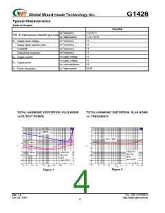
Output power (each channel) see Note
P(OUT)
W
Total harmonic distortion plus noise
THD+N
BOM
m%
Maximum output power bandwidth
Phase margin
Power supply ripple rejection
Channel-to-channel output separation
Input impedance
kHz
°
dB
dB
MΩ
dB
RL = 4Ω, Open Load
f = 120Hz
f = 1kHz
PSRR
ZI
2
90
55
Signal-to-noise ratio
Output noise voltage
PO = 500mW, BTL
Output noise voltage
Vn
µV (rms)
Note :Output power is measured at the output terminals of the IC at 1kHz.
TEL: 886-3-5788833
http://www.gmt.com.tw
Ver: 1.0
Dec 04, 2003
2

 GMT [ GLOBAL MIXED-MODE TECHNOLOGY INC ]