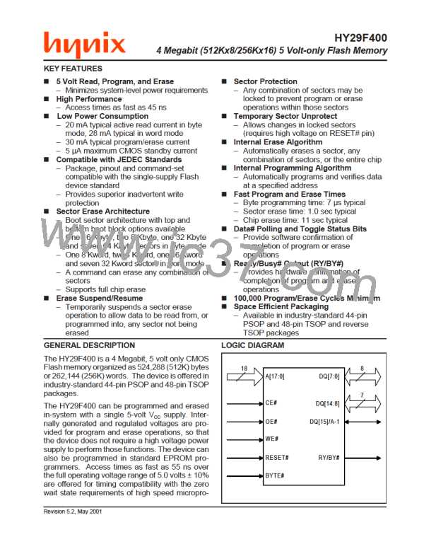
HY29F400
provide any controls or timings during these op-
erations.
internally generated erase pulses and verifies cell
erasure within the proper cell margins. The host
system is not required to provide any controls or
timings during these operations.
Commands written to the device during execution
of the Automatic Erase algorithm are ignored. Note
that a hardware reset immediately terminates the
erase operation. To ensure data integrity, the
aborted Chip Erase command sequence should
be reissued once the reset operation is complete.
After the sector erase data cycle (the sixth bus
cycle) of the command sequence is issued, a sec-
tor erase time-out of 50 µs, measured from the
rising edge of the final WE# pulse in that bus cycle,
begins. During this time, an additional sector erase
data cycle, specifying the sector address of an-
other sector to be erased, may be written into an
internal sector erase buffer. This buffer may be
loaded in any sequence, and the number of sec-
tors specified may be from one sector to all sec-
tors. The only restriction is that the time between
these additional data cycles must be less than 50
µs, otherwise erasure may begin before the last
data cycle is accepted. To ensure that all data
cycles are accepted, it is recommended that host
processor interrupts be disabled during the time
that the additional cycles are being issued and then
be re-enabled afterwards.
When the Automatic Erase algorithm is finished,
the device returns to the Read mode. Several
methods are provided to allow the host to deter-
mine the status of the erase operation, as de-
scribed in the Write Operation Status section.
Figure 5 illustrates the Chip Erase procedure.
Sector Erase Command
The Sector Erase command sequence consists
of two unlock cycles, followed by the erase com-
mand, two additional unlock cycles and then the
sector erase data cycle, which specifies which
sector is to be erased. As described later in this
section, multiple sectors can be specified for era-
sure with a single command sequence. During
sector erase, all specified sectors are erased se-
quentially. The data in sectors not specified for
erasure, as well as the data in any protected secto-
rs, even if specified for erasure, is not affect-
ed by the sector erase operation.
Note: The device is capable of accepting three ways
of invoking Erase Commands for additional sectors
during the time-out window. The preferred method,
described above, is the sector erase data cycle after
the initial six bus cycle command sequence. However,
the device also accepts the following methods of
specifying additional sectors during the sector erase
time-out:
n Repeat the entire six-cycle command sequence,
specifying the additional sector in the sixth cycle.
n Repeat the last three cycles of the six-cycle command
sequence, specifying the additional sector in the third
cycle.
The Sector Erase command sequence starts the
Automatic Erase algorithm, which preprograms
and verifies the specified unprotected sectors for
an all zero data pattern prior to electrical erase.
The device then provides the required number of
If all sectors scheduled for erasing are protected,
the device returns to reading array data after ap-
proximately 100 µs. If at least one scheduled sec-
tor is not protected, the erase operation erases
the unprotected sectors, and ignores the command
for the scheduled sectors that are protected.
START
Issue CHIP ERASE
Command Sequence
The system can monitor DQ[3] to determine if the
50 µs sector erase time-out has expired, as de-
scribed in the Write Operation Status section. If
the time between additional sector erase data
cycles can be insured to be less than the time-
out, the system need not monitor DQ[3].
Check Erase Status
DQ[5] Error Exit
(See Write Operation Status
Section)
Normal Exit
GO TO
CHIP ERASE COMPLETE
Any command other than Sector Erase or Erase
Suspend during the time-out period resets the
device to reading array data. The system must
then rewrite the command sequence, including any
ERROR RECOVERY
Figure 5. Chip Erase Procedure
Rev. 5.2/May 01
13

 HYNIX [ HYNIX SEMICONDUCTOR ]