TDA 4700
TDA 4718
Characteristics (cont’d)
VS = 11 to 30 V; TA = – 25 to 85 °C
Parameter
Symbol
Limit Values
typ. max.
Unit Test
Condition
min.
Comparator K2
Input current
Turn-OFF delay1)
Input voltage
– II K2
tD OFF
VI K2
2
500
µA
ns
for duty cycle
D = 0
D = max.
1.8
5
V
V
Common-mode input
voltage range
VI C
0
5.5
V
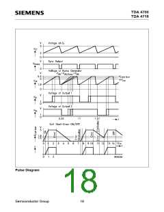
Soft Start K3, K4
Charge current for
Csoft start
Ich
6
µA
Discharge current for
Csoft start
Upper limiting voltage Vlim
Switching voltage K4 VK4
Idch
2
5
1.5
µA
V
V
Operational Amplifier K1 (TDA 4700; TDA 4700 A)
Open-loop voltage
gain
GV0
VIO
60
– 10
80
dB
mV
Input offset voltage
Temperature
10
coefficient of VIO
Input current
TC
– II
– 30
30
2
µV/K
µA
Common-mode input
voltage range
Output current
Rise time of output
voltage
Transition frequency
Phase at fT
VIC
IQ
0
– 3
5
1.5
V
mA
∆V/∆t
fT
ϕT
1
3
120
V/µs
MHz
deg.
V
Output voltage
VQ H/L
1.5
5.5
– 3 mA< I< 1.5 mA
1)
At the input: step function ∆V = – 100 mV
∆V = + 100 mV
Semiconductor Group
14

 INFINEON [ Infineon ]