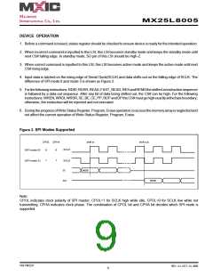
MX25L8005
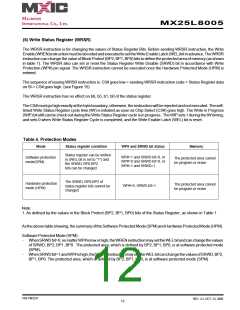
Note: If SRWD bit=1 but WP# is low, it is impossible to write the Status Register even if the WEL bit has previously been
set. It is rejected to write the Status Register and not be executed.
HardwareProtectedMode(HPM):
-
When SRWD bit=1, and then WP# is low (or WP# is low before SRWD bit=1), it enters the hardware protected mode
(HPM). The data of the protected area is protected by software protected mode by BP2, BP1, BP0 and hardware
protected mode by the WP# to against data modification.
Note:toexitthehardwareprotectedmoderequiresWP#drivinghighoncethehardwareprotectedmodeisentered.Ifthe
WP# pin is permanently connected to high, the hardware protected mode can never be entered; only can use software
protected mode via BP2, BP1, BP0.
(6) Read Data Bytes (READ)
Thereadinstructionisforreadingdataout.TheaddressislatchedonrisingedgeofSCLK,anddatashiftsoutonthefalling
edge of SCLK at a maximum frequency fR. The first address byte can be at any location. The address is automatically
increased to the next higher address after each byte data is shifted out, so the whole memory can be read out at a single
READ instruction. The address counter rolls over to 0 when the highest address has been reached.
The sequence of issuing READ instruction is: CS# goes low-> sending READ instruction code-> 3-byte address on SI
-> data out on SO-> to end READ operation can use CS# to high at any time during data out. (see Figure. 16)
(7) Read Data Bytes at Higher Speed (FAST_READ)
The FAST_READ instruction is for quickly reading data out. The address is latched on rising edge of SCLK, and data of
each bit shifts out on the falling edge of SCLK at a maximum frequency fC. The first address byte can be at any location.
Theaddressisautomaticallyincreasedtothenexthigheraddressaftereachbytedataisshiftedout,sothewholememory
can be read out at a single FAST_READ instruction. The address counter rolls over to 0 when the highest address has
beenreached.
The sequence of issuing FAST_READ instruction is: CS# goes low-> sending FAST_READ instruction code-> 3-byte
address on SI-> 1-dummy byte address on SI->data out on SO-> to end FAST_READ operation can use CS# to high at
any time during data out. (see Figure. 17)
While Program/Erase/Write Status Register cycle is in progress, FAST_READ instruction is rejected without any impact
on the Program/Erase/Write Status Register current cycle.
(8) Sector Erase (SE)
TheSectorErase(SE)instructionisforerasingthedataofthechosensectortobe "1".AWriteEnable(WREN)instruction
must execute to set the Write Enable Latch (WEL) bit before sending the Sector Erase (SE). Any address of the sector
(see table 3) is a valid address for Sector Erase (SE) instruction. The CS# must go high exactly at the byte boundary (the
latest eighth of address byte been latched-in); otherwise, the instruction will be rejected and not executed.
Address bits [Am-A12] (Am is the most significant address) select the sector address.
The sequence of issuing SE instruction is: CS# goes low -> sending SE instruction code-> 3-byte address on SI -> CS#
goes high. (see Figure 19)
P/N:PM1237
REV. 2.2, OCT. 23, 2008
13

 Macronix [ MACRONIX INTERNATIONAL ]