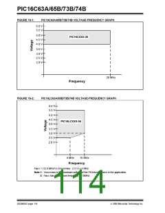
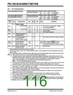
PIC16C63A/65B/73B/74B
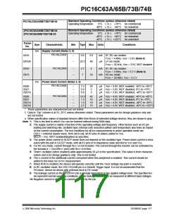
16.1 DC Characteristics
Standard Operating Conditions (unless otherwise stated)
PIC16LC63A/65B/73B/74B-04
Operating temperature
0°C ≤ TA ≤ +70°C for commercial
-40°C ≤ TA ≤ +85°C for industrial
Standard Operating Conditions (unless otherwise stated)
‡PIC16C63A/65B/73B/74B-04
‡PIC16C6A/65B/73B/74B-20
Operating temperature
0°C ≤ TA ≤ +70°C for commercial
-40°C ≤ TA ≤ +85°C for industrial
-40°C ≤ TA ≤ +125°C for extended
Param
No.
Sym
Characteristic
Min
Typ† Max
Units
Conditions
VDD Supply Voltage
PIC16LCXXX
D001
2.5
VBOR*
–
–
5.5
5.5
V
V
LP, XT, RC osc modes (DC - 4 MHz)
BOR enabled (Note 7)
PIC16CXXX
D001
D001A
4.0
4.5
VBOR*
–
–
–
5.5
5.5
5.5
V
V
V
XT, RC and LP osc mode
HS osc mode
BOR enabled (Note 7)
D002*
D003
VDR RAM Data Retention
–
–
1.5
–
V
Voltage (Note 1)
VPOR VDD Start Voltage to
ensure internal
VSS
–
V
See section on Power-on Reset for details
Power-on Reset signal
D004*
D004A*
SVDD VDD Rise Rate to
ensure internal
0.05
TBD
–
–
–
–
V/mS PWRT enabled (PWRTE bit clear)
V/mS PWRT disabled (PWRTE bit set)
See section on Power-on Reset for details
Power-on Reset signal
D005
VBOR Brown-out Reset
3.65
–
4.35
V
BODEN bit set
voltage trip point
* These parameters are characterized but not tested.
† Data in “Typ” column is at 5V, 25°C unless otherwise stated. These parameters are for design guidance only and
are not tested.
‡ When specification values of standard devices differ from those of extended voltage devices, they are shown in gray.
Note 1: This is the limit to which VDD can be lowered without losing RAM data.
2: The supply current is mainly a function of the operating voltage and frequency. Other factors such as I/O pin
loading and switching rate, oscillator type, internal code execution pattern and temperature also have an impact
on the current consumption. The test conditions for all IDD measurements in active operation mode are:
OSC1 = external square wave, from rail to rail; all I/O pins tri-stated, pulled to VDD,
MCLR = VDD; WDT enabled/disabled as specified.
3: The power-down current in SLEEP mode does not depend on the oscillator type. Power-down current is mea-
sured with the part in SLEEP mode, with all I/O pins in hi-impedance state and tied to VDD and VSS.
4: For RC osc mode, current through REXT is not included. The current through the resistor can be estimated by
the formula Ir = VDD/2REXT (mA) with REXT in kOhm.
5: Timer1 oscillator (when enabled) adds approximately 20 µA to the specification. This value is from character-
ization and is for design guidance only. This is not tested.
6: The ∆ current is the additional current consumed when this peripheral is enabled. This current should be
added to the base IDD or IPD measurement.
7: When BOR is enabled, the device will operate correctly until the VBOR voltage trip point is reached.
8: In RC oscillator mode, the OSC1/CLKIN pin is a Schmitt Trigger input. It is not recommended that the
PICmicro device be driven with external clock in RC mode.
9: The leakage current on the MCLR/VPP pin is strongly dependent on the applied voltage level. The specified lev-
els represent normal operating conditions. Higher leakage current may be measured at different input voltages.
10:Negative current is defined as current sourced by the pin.
DS30605C-page 116
2000 Microchip Technology Inc.

 MICROCHIP [ MICROCHIP ]