ISO-CMOS MT8952B
an "all-call". The LSB of the Receiver Address
Register is set LOW permanently and the address
comparison is done only on remaining bits of the
register.
state during that period. However, the C-channel
information is received independently and the C-
channel Status Register is updated continuously.
Note that C1EN has relevance only during the
Internal Timing Mode.
C-Channel Control Register (Read/Write):
BRCK- Bit Rate Clock: This bit is used during the
Internal Timing Mode to select the clock rate and
ignored if the Protocol Controller is in the External
Timing Mode. It should be set HIGH if the input clock
(CKi) is at the bit rate (C2i) and should be LOW for
the clock input at 2 x bit rate (C4i). In both cases,
the clock should be properly phase related to F0i as
shown in Figure 25.
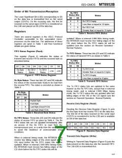
D7
D6
D5
D4
D3
D2
D1
D0
CT7
CT6
CT5
CT4
CT3
CT2
CT1
CT0
Figure 9 - C-Channel Control Register
The data written to this register (Figure 9) is
transmitted on channel-1 slot of the outgoing ST-
BUS (CDSTo), when enabled by C1EN bit in the
Timing Control Register. This feature can only be
used when the HDLC Protocol Controller is in the
Internal Timing Mode.
TC0-TC3 - Timing Control Bits: In the Internal
Timing Mode the transmitter and the receiver
sections are enabled during the times defined by the
Timing Control Bits TC0-TC3 (Table 7). This applies
only to the ST-BUS channels 0, 2, 3 and 4 carrying
the packets or transparent data (channel-1 pertains
to C-channel information). The output CDSTo is put
during the remaining time intervals not enabled by
these bits.
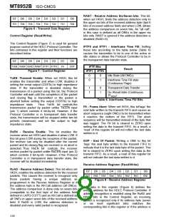
Timing Control Register (Read/Write):
The Timing Control Register (Figure 10) controls the
timing mode and other related operations and
provides a software reset to the Protocol Controller.
The various bits in this register are described below:
D7
D6
D5
D4
D3
D2
D1
D0
Timing Control Bits
ST-BUS
Channel
Number
Bits
RST
IC
C1EN BRCK TC3
TC2
TC1
TC0
/Frame
TC3 TC2 TC1 TC0
Figure 10. Timing Control Register
X
X
0
0
0
0
0
0
1
1
1
1
0
0
1
1
1
0
0
1
1
0
1
0
0
1
0
1
0
1
0
1
2
0
RST - Reset: When this bit is set HIGH, all the
registers in the HDLC Protocol Controller are reset
and the data in the FIFOs is lost. This is equivalent to
the external reset with the exception that the RST bit
does not affect itself or the Watchdog Timer Register
and WD output. The RST bit must be “cleared”
(written as a logic “0”) twice before the MT8952B will
be removed from its reset state (see section on
RESET operation).
0
6
1
0
7
X
X
X
X
X
2
8
3
4
8
8
2 and 3
2, 3 and 4
16
24
X : Don’t Care Table 7. Timing Control Bits
IC - Internal Control: When this bit is cleared to
ZERO, the Protocol Controller is in the External
Timing Mode. The transmit and receive sections are
enabled by the inputs TxCEN and RxCEN
respectively, and F0i is used only for the watchdog
timer operation. When this bit is a ONE, the Protocol
Controller is in the Internal Timing Mode. The
transmit and receive sections are enabled by the
internally generated timings derived from the inputs
CKi and F0i. The F0i input defines the beginning of a
frame (Figure 24) and the transmitter and receiver
sections are enabled in the timeslots as determined
by the bits TCO-TC3. The inputs TxCEN and RxCEN
are ignored in this mode.
Interrupt Flag Register (Read):
Reading the Interrupt Flag Register puts the interrupt
status bits on the data bus. This register is reset
when it is read and a particular bit will not be set until
its particular condition occurs again. The functional
details of each bit are provided in Figure 11.
D7
D6
D5
D4
D3
D2
D1
Rx
D0
Rx
OFLW
GA EOPD
Tx
FA
Tx
Tx
DONE
4/19 URUN 15/19
FULL FULL
Figure 11. Interrupt Flag Register
GA - Go Ahead: This bit when set HIGH, indicates
the detection of ‘go ahead’ sequence on the
incoming data stream (CDSTi).
C1EN - Channel-1 Enable: When HIGH, it enables
the transmission of C-channel information on
channel-1 time-slot of the outgoing ST-BUS (CDSTo)
and when LOW, puts CDSTo into high impedance
3-69

 MITEL [ MITEL NETWORKS CORPORATION ]