Advance Information
MT9041B
Pin Description (continued)
Pin #
Name
Description
19
20
21
22
23
IC0
IC1
IC0
IC0
MS
Internal Connect. Connect to Vss
Internal Connect. Leave open Circuit
Internal Connect. Connect to Vss
Internal Connect. Connect to Vss
Mode/Control Select (TTL Input). This pin, determines the device’s state (Normal, or
Freerun) of operation. The logic level at this input is gated in by the rising edge of F8o. See
Table 3.
24
25
26
IC0
IC0
FS2
Internal Connect. Connect to Vss
Internal Connect. Connect to Vss
Frequency Select 2 (TTL Input). This input, in conjunction with FS1, selects which of three
possible frequencies (8kHz, 1.544MHz, or 2.048MHz) may be input to the REF input. See
Table 1.
27
28
FS1
RST
Frequency Select 1 (TTL Input). See pin description for FS2.
Reset (Schmitt Input). A logic low at this input resets the MT9041B. To ensure proper
operation, the device must be reset after reference signal frequency changes and power-up.
The RST pin should be held low for a minimum of 300ns. While the RST pin is low, all frame
and clock outputs are at logic high. Following a reset, the input reference source and output
clocks and frame pulses are phase aligned as shown in Figure 10.
Functional Description
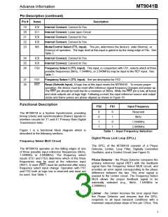
FS2
FS1
Input Frequency
0
0
1
1
0
1
0
1
Reserved
8kHz
The MT9041B is a System Synchronizer, providing
timing (clock) and synchronization (frame) signals to
interface circuits for T1 and E1 Primary Rate Digital
Transmission links.
1.544MHz
2.048MHz
Figure 1 is a functional block diagram which is
described in the following sections.
Table 1 - Input Frequency Selection
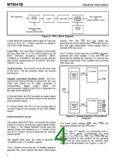
Digital Phase Lock Loop (DPLL)
Frequency Select MUX Circuit
The DPLL of the MT9041B consists of a Phase
Detector, Limiter, Loop Filter, Digitally Controlled
Oscillator, and a Control Circuit (see Figure 3).
The MT9041B operates on the falling edges of one
of three possible input reference frequencies (8kHz,
1.544MHz or 2.048MHz). The frequency select
inputs (FS1 and FS2) determine which of the three
frequencies may be used at the reference input
(REF). A reset (RST) must be performed after every
frequency select input change. Operation with FS1
and FS2 both at logic low is reserved and must not
be used. See Table 1.
Phase Detector - the Phase Detector compares the
primary reference signal (REF) with the feedback
signal from the Frequency Select MUX circuit, and
provides an error signal corresponding to the phase
difference between the two. This error signal is
passed to the Limiter circuit. The Frequency Select
MUX allows the proper feedback signal to be
externally selected (e.g., 8kHz, 1.544MHz or
2.048MHz).
Limiter - the Limiter receives the error signal from
the Phase Detector and ensures that the DPLL
responds to all input transient conditions with a
maximum output phase slope of 5ns per 125us. This
3

 MITEL [ MITEL NETWORKS CORPORATION ]