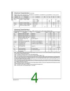
Electrical Characteristics (Continued)
Digital Levels and DC Specifications: ADC0808CCN, ADC0808CCV, ADC0809CCN and ADC0809CCV, 4.75≤VCC≤5.25V,
−40˚C≤TA≤+85˚C unless otherwise noted
Symbol
Parameter
Conditions
Min
Typ
Max
Units
DATA OUTPUTS AND EOC (INTERRUPT)
=
VCC 4.75V
VOUT(1)
Logical “1” Output Voltage
=
IOUT −360µA
2.4
4.5
V(min)
V(min)
=
IOUT −10µA
=
VOUT(0)
VOUT(0)
IOUT
Logical “0” Output Voltage
Logical “0” Output Voltage EOC
TRI-STATE Output Current
IO 1.6 mA
0.45
0.45
3
V
V
=
IO 1.2 mA
=
VO 5V
µA
µA
=
VO
0
−3
Electrical Characteristics
=
=
=
= =
=
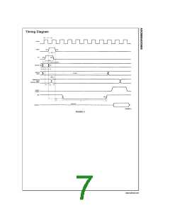
Timing Specifications VCC VREF(+) 5V, VREF(−) GND, tr tf 20 ns and TA 25˚C unless otherwise noted.
Symbol
tWS
tWALE
ts
Parameter
Minimum Start Pulse Width
Minimum ALE Pulse Width
Minimum Address Set-Up Time
Minimum Address Hold Time
Analog MUX Delay Time
From ALE
Conditions
MIn
Typ
100
100
25
Max
200
200
50
Units
ns
(Figure 5)
(Figure 5)
(Figure 5)
(Figure 5)
ns
ns
tH
25
50
ns
=
tD
RS 0Ω (Figure 5)
1
2.5
µs
=
=
t
t
H1, tH0
1H, t0H
OE Control to Q Logic State
OE Control to Hi-Z
CL 50 pF, RL 10k (Figure 8)
125
125
100
640
250
250
ns
ns
=
=
CL 10 pF, RL 10k (Figure 8)
=
tc
Conversion Time
fc 640 kHz, (Figure 5) (Note 7)
90
10
0
116
µs
fc
Clock Frequency
1280
8+2 µS
kHz
Clock
Periods
pF
tEOC
EOC Delay Time
(Figure 5)
CIN
Input Capacitance
TRI-STATE Output
Capacitance
At Control Inputs
10
10
15
15
COUT
At TRI-STATE Outputs
pF
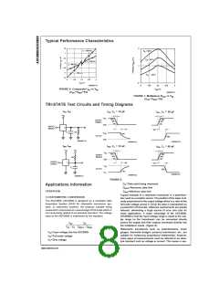
Note 1: Absolute Maximum Ratings indicate limits beyond which damage to the device may occur. DC and AC electrical specifications do not apply when operating
the device beyond its specified operating conditions.
Note 2: All voltages are measured with respect to GND, unless othewise specified.
Note 3: A zener diode exists, internally, from V
CC
to GND and has a typical breakdown voltage of 7 V .
DC
Note 4: Two on-chip diodes are tied to each analog input which will forward conduct for analog input voltages one diode drop below ground or one diode drop greater
than the V n supply. The spec allows 100 mV forward bias of either diode. This means that as long as the analog V does not exceed the supply voltage by more
C
C
I
N
than 100 mV, the output code will be correct. To achieve an absolute 0V to 5V input voltage range will therefore require a minimum supply voltage of 4.900 V
DC DC DC
over temperature variations, initial tolerance and loading.
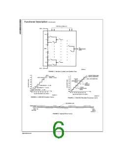
Note 5: Total unadjusted error includes offset, full-scale, linearity, and multiplexer errors. See Figure 3. None of these A/Ds requires a zero or full-scale adjust. How-
ever, if an all zero code is desired for an analog input other than 0.0V, or if a narrow full-scale span exists (for example: 0.5V to 4.5V full-scale) the reference voltages
can be adjusted to achieve this. See Figure 13.
Note 6: Comparator input current is a bias current into or out of the chopper stabilized comparator. The bias current varies directly with clock frequency and has little
temperature dependence (Figure 6). See paragraph 4.0.
Note 7: The outputs of the data register are updated one clock cycle before the rising edge of EOC.
Note 8: Human body model, 100 pF discharged through a 1.5 kΩ resistor.
www.national.com
4

 NSC [ National Semiconductor ]