M25P32
Instructions
6.4.4
SRWD bit
The Status Register Write Disable (SRWD) bit is operated in conjunction with the Write
Protect (W/V ) signal. The Status Register Write Disable (SRWD) bit and Write Protect
PP
(W/V ) signal allow the device to be put in the Hardware Protected mode (when the Status
PP
Register Write Disable (SRWD) bit is set to 1, and Write Protect (W/V ) is driven Low). In
PP
this mode, the non-volatile bits of the Status Register (SRWD, BP2, BP1, BP0) become
read-only bits and the Write Status Register (WRSR) instruction is no longer accepted for
execution.
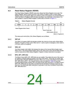
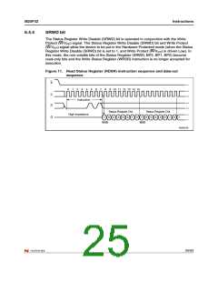
Figure 11. Read Status Register (RDSR) instruction sequence and data-out
sequence
S
0
1
2
3
4
5
6
7
8
9 10 11 12 13 14 15
C
D
Instruction
Status Register Out
Status Register Out
High Impedance
Q
7
6
5
4
3
2
1
0
7
6
5
4
3
2
1
0
7
MSB
MSB
AI02031E
25/53

 NUMONYX [ NUMONYX B.V ]