DC and AC parameters
M25P32
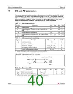
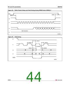
10
DC and AC parameters
This section summarizes the operating and measurement conditions, and the DC and AC
characteristics of the device. The parameters in the DC and AC Characteristic tables that
follow are derived from tests performed under the Measurement Conditions summarized in
the relevant tables. Designers should check that the operating conditions in their circuit
match the measurement conditions when relying on the quoted parameters.
Table 10. Operating conditions
Symbol
Parameter
Min.
Typ.
Max. Unit
VCC
Supply voltage
2.7
3.6
9.5
85
V
V
Supply voltage on W/VPP pin for Fast Program/Erase
mode
VPPH
TA
8.5
–40
15
Ambient operating temperature
°C
°C
Ambient operating temperature for fast Program/Erase
mode
TAVPP
25
35
Table 11. AC measurement conditions
Symbol
Parameter
Min.
Max.
Unit
CL
Load capacitance
30
pF
ns
V
Input rise and fall times
5
Input pulse voltages
0.2VCC to 0.8VCC
0.3VCC to 0.7VCC
Input timing reference voltages
Output timing reference voltages
V
V
CC / 2
V
1. Output Hi-Z is defined as the point where data out is no longer driven.
Figure 22. AC measurement I/O waveform
Input Levels
Input and Output
Timing Reference Levels
0.8V
CC
0.7V
CC
0.5V
CC
0.3V
CC
0.2V
CC
AI07455
(1)
Table 12. Capacitance
Symbol
Parameter
Test condition
Min.
Max.
Unit
COUT
CIN
Output capacitance (Q)
VOUT = 0 V
VIN = 0 V
8
6
pF
pF
Input capacitance (other pins)
1. Sampled only, not 100% tested, at TA=25 °C and a frequency of 20 MHz.
40/53

 NUMONYX [ NUMONYX B.V ]