FEDL2250DIGEST-01
OKI Semiconductor
ML2252/54-XXX, ML22Q54
PIN DESCRIPTIONS-2
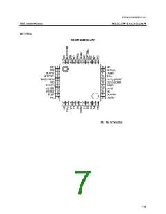
ML22Q54 Pins
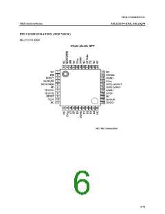
44-pin plastic QFP
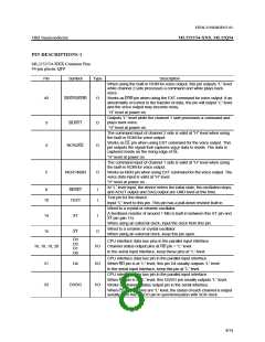
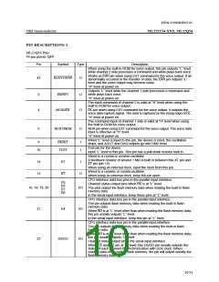
Pin
43
Symbol
Type
O
Description
When using the built-in ROM for voice output, this pin outputs “L” level
while channel 2 side processes a command and while plays back voice.
Works as ERR pin when using EXT command for the voice output. If an
abnormality occurred in the transfer of data, the ERR pin outputs “L”
level and the voice output may become noisy.
BUSY2/ERR
“H” level at power on.
Outputs “L” level while the channel 1 side processes a command and
while plays back voice.
“H” level at power on.
3
4
BUSY1
O
O
The input command of channel 2 is valid at “H” level when using the
built-in ROM for voice output.
NCR2/DL
DL pin when using EXT command for the voice output. It outputs the
voice data capture signal. The data is captured on the rising edge of DL.
“H” level at power on.
The command input of channel 1 side is valid at “H” level when using
the built-in ROM for voice output.
5
NCR1/NDR
O
NDR pin when using EXT command for the voice output. The voice data
input is effective at “H” level.
“H” level at power on.
When “L” level is input to this pin, the device is reset, the oscillation
stops, and AOUT and DAQ outputs go into GND level.
9
RESET
I
I
Test pin for the device.
Input “L” level to this pin. This pin has a pull-down resistor built in.
Wired to a crystal or ceramic oscillator.
10
TEST
A feedback resistor of around 1 MΩ is built in between this XT pin and
XT pin (pin 15).
14
15
XT
I
When using an external clock, input the clock from this pin.
Wired to a ceramic or crystal oscillator.
XT
O
When using an external clock, keep this pin open.
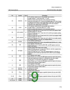
CPU interface data bus pins in the parallel input interface.
Channel status output pins when RD is at “L” level.
The pins output the flash memory data when reading the built-in flash
memory data.
In the serial input interface, keep these pins at “L” level.
CPU interface data bus pin in the parallel input interface.
The pin outputs flash memory data when reading the built-in flash
memory data.
D3
D2
D1
D0
16, 18, 19, 20
I/O
I/O
21
D4
When RD is at “L” level other than when reading the flash memory data,
this pin usually outputs “L” level.
In the serial input interface, keep this pin at “L” level.
CPU interface data bus pin in the parallel input interface.
The pin outputs flash memory data when reading the built-in flash
memory data.
When RD is at “L” level other than when reading the flash memory data,
this pin usually outputs “L” level.
Channel status output pin in the serial input interface.
23
D5/DO
I/O
When CS and RD are at “L” level, this D5/DO pin serially outputs the
status of each channel in synchronization with SCK clock. When
reading data of the built-in flash memory, the pin will output serially the
flash memory data.
10/31

 OKI [ OKI ELECTRONIC COMPONETS ]