LNK362-364
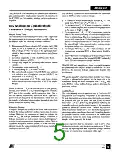
Input Filter
Capacitor
TOP VIEW
Y1-
Capacitor
FB
D
T
r
a
n
s
f
o
r
m
e
r
S
S
BP
S
S
+
-
HV DC
INPUT
S
S
CBP
Opto-
coupler
+
DC
Maximize hatched copper
OUT
areas (
) for optimum
-
heatsinking
Output Filter
Capacitor
PI-4155-102705
Figure 6. Recommended Printed Circuit Layout for LinkSwitch-XT in a Flyback Converter Configuration.
LinkSwitch-XT Layout Considerations
(~200 V) and diode clamp across the primary winding. In all
cases, to minimize EMI, care should be taken to minimize the
circuit path from the clamp components to the transformer and
LinkSwitch-XT.
See Figure 6 for a recommended circuit board layout for
LinkSwitch-XT.
Single Point Grounding
Thermal Considerations
Use a single point ground connection from the input filter
capacitor to the area of copper connected to the SOURCE
pins.
The copper area underneath the LinkSwitch-XT acts not only
as a single point ground, but also as a heatsink. As this area is
connected to the quiet source node, it should be maximized for
good heat sinking of LinkSwitch-XT. The same applies to the
cathode of the output diode.
Bypass Capacitor CBP
TheBYPASSpincapacitorshouldbelocatedasnearaspossible
to the BYPASS and SOURCE pins.
Y Capacitor
The placement of the Y capacitor should be directly from
the primary input filter capacitor positive terminal to the
common/return terminal of the transformer secondary. Such
a placement will route high magnitude common-mode surge
currents away from the LinkSwitch-XT device. Note that if an
input pi (C, L, C) EMI filter is used, then the inductor in the
filter should be placed between the negative terminals of the
input filter capacitors.
Primary Loop Area
The area of the primary loop that connects the input filter
capacitor, transformer primary and LinkSwitch-XT together
should be kept as small as possible.
Primary Clamp Circuit
Aclamp is used to limit peak voltage on the DRAIN pin at turn
off. This can be achieved by using an RCD clamp or a Zener
C
12/05
6

 POWERINT [ Power Integrations ]