TNY263-268
Design
Key Application Considerations
TinySwitch-II vs. TinySwitch
Output Power
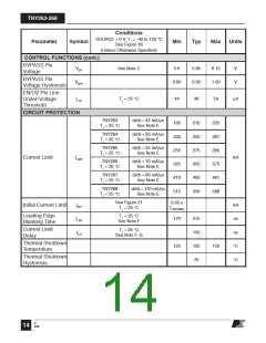
Table1(frontpage)showsthepracticalcontinuousoutputpower
levels that can be obtained under the following conditions:
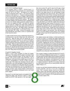
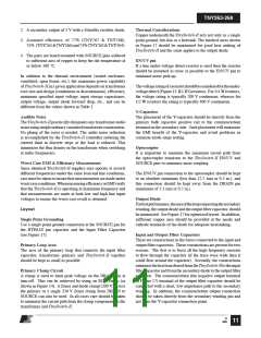
Table 2 compares the features and performance differences
between the TNY254 device of the TinySwitch family with
the TinySwitch-II family of devices. Many of the new features
eliminate the need for or reduce the cost of circuit components.
Other features simplify the design and enhance performance.
1. The minimum DC input voltage is 90 V or higher for
85 VAC input, or 240 V or higher for 230 VAC input or
115 VAC input with a voltage doubler. This corresponds to
a filter capacitor of 3 µF/W for universal input and 1 µF/W
for 230 VAC or 115 VAC with doubler input.
TinySwitch
TinySwitch-II
TNY263-268
TinySwitch-II
Advantages
Function
TNY254
Switching Frequency
and Tolerance
44 kHz ±10% (at 25 °C) 132 kHz ±6% (at 25 °C) • Smaller transformer for low cost
• Ease of design
Temperature Variation
(0-100 °C)**
+8%
N/A*
N/A*
+2%
• Manufacturability
• Optimum design for lower cost
Active Frequency Jitter
±4 kHz
• Lower EMI minimizing filter
component costs
Transformer Audible
Noise Reduction
Yes–built into controller • Practically eliminates audible
noise with ordinary dip varnished
transformer – no special
construction or gluing required
Line UV Detect
N/A*
Single resistor
programmable
• Prevents power on/off glitches
Current Limit Tolerance ±11% (at 25 °C)
±7% (at 25 °C)
0%
• Increases power capability and
simplifies design for high volume
manufacturing
Temperature Variation
-8%
(0-100 °C)**
Auto-Restart
N/A*
6% effective on-time
• Limits output short-circuit current
to less than full load current
- No output diode size penalty
• Protects load in open loop fault
conditions
- No additional components
required
BYPASS Pin Zener
Clamp
N/A*
Internally clamped to
6.3 V
• Allows TinySwitch-II to be
powered from a low voltage bias
winding to improve efficiency and
to reduce on-chip power
dissipation
DRAIN Creepage at
Package
0.037 in. / 0.94 mm
0.137 in. / 3.48 mm
• Greater immunity to arcing as a
result of dust, debris or other
contaminants build-up
*Not available.
** See typical performance curves.
Table 2. Comparison Between TinySwitch and TinySwitch-II.
G
4/05
10

 POWERINT [ Power Integrations ]