TNY263-268
BYPASS
(BP)
DRAIN
(D)
REGULATOR
5.8 V
LINE UNDER-VOLTAGE
240 µA
50 µA
FAULT
PRESENT
BYPASS PIN
UNDER-VOLTAGE
+
-
AUTO-
RESTART
COUNTER
5.8 V
4.8 V
CURRENT
LIMIT STATE
MACHINE
V
I
LIMIT
RESET
6.3 V
CURRENT LIMIT
COMPARATOR
-
ENABLE
+
JITTER
CLOCK
1.0 V + V
THERMAL
SHUTDOWN
T
DC
MAX
OSCILLATOR
ENABLE/
UNDER-
VOLTAGE
(EN/UV)
1.0 V
S
Q
Q
R
LEADING
EDGE
BLANKING
SOURCE
(S)
PI-2643-030701
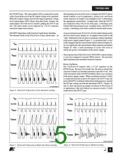
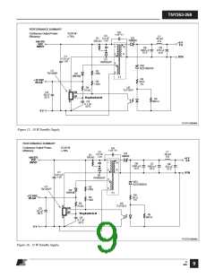
Figure 2. Functional Block Diagram.
Pin Functional Description
P Package (DIP-8B)
G Package (SMD-8B)
DRAIN (D) Pin:
Power MOSFETdrain connection. Provides internal operating
current for both start-up and steady-state operation.
BP
S
S (HV RTN)
S (HV RTN)
1
2
8
7
BYPASS (BP) Pin:
Connection point for a 0.1 µF external bypass capacitor for the
internally generated 5.8 V supply.
S
3
4
EN/UV
5
ENABLE/UNDER-VOLTAGE (EN/UV) Pin:
D
Thispinhasdualfunctions:enableinputandlineunder-voltage
sense. During normal operation, switching of the power
MOSFET is controlled by this pin. MOSFET switching is
terminated when a current greater than 240 µA is drawn from
this pin. This pin also senses line under-voltage conditions
through an external resistor connected to the DC line
voltage. If there is no external resistor connected to this pin,
TinySwitch-II detects its absence and disables the line under-
voltage function.
PI-2685-101600
Figure 3. Pin Configuration.
SOURCE (S) Pin:
Control circuit common, internally connected to output
MOSFET source.
SOURCE (HV RTN) Pin:
Output MOSFET source connection for high voltage return.
G
4/05
2

 POWERINT [ Power Integrations ]