TNY274-280
200
100
V
V
EN
DC-INPUT
0
CLOCK
10
DC
MAX
V
5
0
BYPASS
I
400
200
0
DRAIN
V
DRAIN
1
2
0
Time (ms)
V
Figure 11. Power-Up Without Optional External UV Resistor
Connected to EN/UV Pin.
DRAIN
PI-2661-082305
200
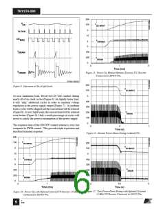
Figure 9. Operation at Very Light Load.
V
100
0
DC-INPUT
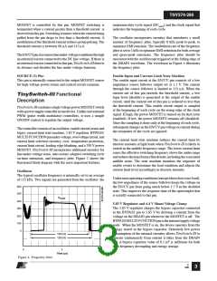
At near maximum load, TinySwitch-III will conduct during
nearly all of its clock cycles (Figure 6). At slightly lower load,
it will “skip” additional cycles in order to maintain voltage
regulation at the power supply output (Figure 7). At medium
loads,cycleswillbeskippedandthecurrentlimitwillbereduced
(Figure 8).At very light loads, the current limit will be reduced
even further (Figure 9). Only a small percentage of cycles will
occur to satisfy the power consumption of the power supply.
400
300
V
200
100
0
DRAIN
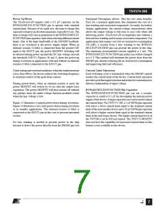
The response time of the ON/OFF control scheme is very fast
compared to PWM control. This provides tight regulation and
excellent transient response.
.5
1
0
Time (s)
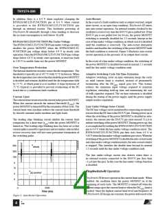
Figure 12. Normal Power-Down Timing (without UV).
200
V
100
200
DC-INPUT
V
0
100
0
DC-INPUT
10
V
5
400
300
BYPASS
0
V
400
200
100
0
DRAIN
200
V
DRAIN
0
1
2
2.5
5
0
0
Time (s)
Time (ms)
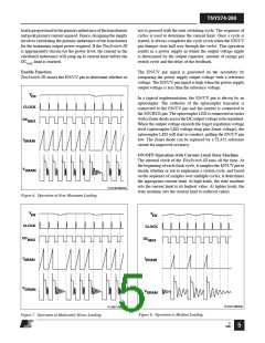
Figure 13. Slow Power-Down Timing with Optional External
Figure 10. Power-Up with Optional External UV Resistor (4 MΩ)
(4 MΩ) UV Resistor Connected to EN/UV Pin.
Connected to EN/UV Pin.
E
2/06
6

 POWERINT [ Power Integrations ]