MITSUBISHI MICROCOMPUTERS
M37905F8CFP, M37905F8CSP
16-BIT CMOS MICROCOMPUTER
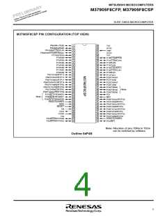
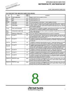
PIN DESCRIPTION (MICROCOMPUTER MODE)
Input/
Output
Pin
Vcc, Vss
MD0
Name
Power supply input
MD0
Functions
Apply 5 V±0.5 V to Vcc, and 0 V to Vss.
—
Input
Input
Connect this pin to VSS.
MD1
MD1
Connect this pin to Vss.
RESET
XIN
Reset input
Clock input
Clock output
Input
The microcomputer is reset when “L” level is applies to this pin.
Input
These are input and output pins of the internal clock generating circuit. Connect a
ceramic resonator or quartz-crystal oscillator between pins XIN and XOUT. When an
external clock is used, the clock source should be connected to pin XIN, and pin
XOUT should be left open.
XOUT
Output
—
—
VCONT
Filter circuit connection
When using the PLL frequency multiplier, connect this pin to the filter circuit. When
not using the PLL frequency multiplier, this pin should be left open.
AVcc,
AVss
Analog power supply input
Power supply input pins for the A-D and D-A converters. Connect AVcc to Vcc, and
AVss to Vss externally.
VREF
Reference voltage input
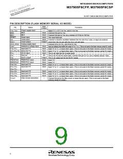
I/O port P1
Input
I/O
This is the reference voltage input pin for the A-D and D-A converters.
P10–P17
Port P1 is an 8-bit I/O port. This port has an I/O direction register, and each pin can
be programmed for input or output. These pins enter the input mode ar reset. These
pins also function as I/O pins of UART0, 1.
P20–P27
P40–P47
I/O port P2
I/O
In addition to having the same functions as port P1, these pins function as I/O pins
for timers A4 and A9. Also, they can be programmed to function as input pins for tim-
ers B0 to B2.
I/O port P4
I/O port P5
I/O
I/O
In addition to having the same functions as port P1, these pins function as I/O pins
for timers A5 to A8. Also, they function as output pins for motor drive waveform.
P51–P53,
P55–P57
In addition to having the same functions as port P1, these pins function as input pins
for INT1 to INT3 and INT5 to INT7. Also, pins P55 to P57 function as input pins for tim-
ers B0 to B2 and as input pins for position data in the three-phase waveform mode;
and pins P52 and P53 function as trigger-input pins in the pulse output port mode.
P60–P67
P70–P77
P80–P83
I/O port P6
I/O port P7
I/O port P8
I/O
I/O
I/O
In addition to having the same functions as port P1, these pins function as I/O pins
for timers A0 to A3. Also, they function as motor drive waveform output pins.
In addition to having the same functions as port P1, these pins function as input pins
for the A-D converter. Also, P77 functions as an output pin for the D-A converter.
In addition to having the same functions as port P1, these pins function as input pins
for the A-D converter. Also, these pins function as I/O pins for UART2, and pin P80
functions as an output pin for the D-A converter.
P4OUTCUT P4OUTCUT input
P6OUTCUT P6OUTCUT input
Input
Input
This pin has the function to forcibly place port P4 pins in the input mode. Also, this
pin functions as an input pin for INT0; and this pin is used to input a signal, which
forcibly cuts off a motor drive waveform output.
This pin has the function to forcibly place port P6 pins in the input mode. Also, this
pin functions as an input pin for INT4; and this pin is used to input a signal, which
forcibly cuts off a motor drive waveform output.
7

 RENESAS [ RENESAS TECHNOLOGY CORP ]