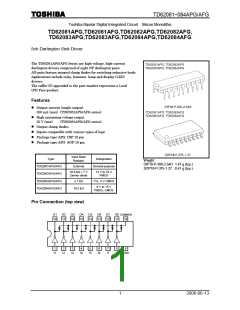
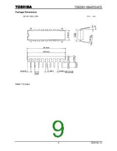
TD62081~084APG/AFG
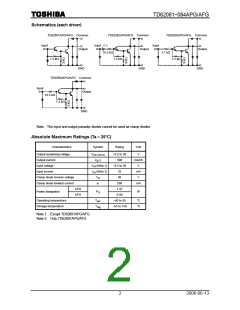
Schematics (each driver)
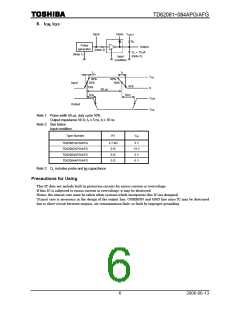
TD62081APG/AFG Common
TD62082APG/AFG Common
Output
TD62083APG/AFG Common
Input
Input
Input
7 V
10.5 kΩ
Output
Output
2.7 kΩ
7.2 kΩ
7.2 kΩ
7.2 kΩ
GND
GND
GND
TD62084APG/AFG Common
Input
Output
10.5 kΩ
7.2 kΩ
GND
Note: The input and output parasitic diodes cannot be used as clamp diodes.
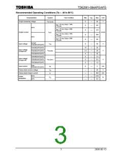
Absolute Maximum Ratings (Ta = 25°C)
Characteristics
Symbol
Rating
Unit
Output sustaining voltage
Output current
V
−0.5 to 50
500
V
mA/ch
V
CE (SUS)
I
OUT
Input voltage
V
IN
I
IN
(Note 1)
−0.5 to 30
25
Input current
(Note 2)
mA
V
Clamp diode reverse voltage
Clamp diode forward current
V
50
R
I
500
mA
F
APG
AFG
1.47
Power dissipation
P
W
D
0.96
Operating temperature
Storage temperature
T
−40 to 85
−55 to 150
°C
°C
opr
T
stg
Note 1: Except TD62081APG/AFG
Note 2: Only TD62081APG/AFG
2
2006-06-13

 TOSHIBA [ TOSHIBA ]