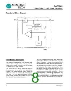
AAT3200
OmniPower™ LDO Linear Regulator
PD(8.2%D/C) = %DC x PD(150mA)
PD(8.2%D/C) = 0.082 x 180mW
PD(8.2%D/C) = 14.8mW
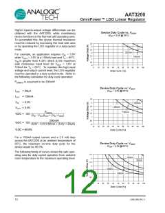
High Peak Output Current Applications
Some applications require the LDO regulator to
operate at continuous nominal levels with short
duration, high-current peaks. The duty cycles for
both output current levels must be taken into
account. To do so, one would first need to calcu-
late the power dissipation at the nominal continu-
ous level, then factor in the addition power dissi-
pation due to the short duration, high-current
peaks.
The power dissipation for a 150mA load occurring
for 8.2% of the duty cycle will be 14.8mW. Finally,
the two power dissipation levels can be summed to
determine the total power dissipation under the
varied load.
PD(total) = PD(100mA) + PD(150mA)
PD(total) = 110.2mW + 14.8mW
PD(total) = 125.0mW
For example, a 3.0V system using a AAT3200IGV-
2.5-T1 operates at a continuous 100mA load cur-
rent level and has short 150mA current peaks. The
current peak occurs for 378µs out of a 4.61ms peri-
od. It will be assumed the input voltage is 5.0V.
The maximum power dissipation for the AAT3200
operating at an ambient temperature of 85°C is
200mW. The device in this example will have a
total power dissipation of 125.0mW. This is well
within the thermal limits for safe operation of the
device.
First the current duty cycle percentage must be
calculated:
% Peak Duty Cycle: X/100 = 378µs/4.61ms
% Peak Duty Cycle = 8.2%
Printed Circuit Board Layout
Recommendations
The LDO regulator will be under the 100mA load for
91.8% of the 4.61ms period and have 150mA peaks
occurring for 8.2% of the time. Next, the continuous
nominal power dissipation for the 100mA load should
be determined then multiplied by the duty cycle to
conclude the actual power dissipation over time.
In order to obtain the maximum performance from
the AAT3200 LDO regulator, very careful attention
must be paid in regard to the printed circuit board
layout. If grounding connections are not properly
made, power supply ripple rejection and LDO regu-
lator transient response can be compromised.
PD(MAX) = (VIN - VOUT)IOUT + (VIN x IGND
)
The LDO regulator external capacitors CIN and
COUT should be connected as directly as possible
to the ground pin of the LDO regulator. For maxi-
mum performance with the AAT3200, the ground
pin connection should then be made directly back
to the ground or common of the source power sup-
ply. If a direct ground return path is not possible
due to printed circuit board layout limitations, the
LDO ground pin should then be connected to the
common ground plane in the application layout.
PD(100mA) = (4.2V - 3.0V)100mA + (4.2V x 20µA)
PD(100mA) = 120mW
PD(91.8%D/C) = %DC x PD(100mA)
PD(91.8%D/C) = 0.918 x 120mW
PD(91.8%D/C) = 110.2mW
The power dissipation for 100mA load occurring for
91.8% of the duty cycle will be 110.2mW. Now the
power dissipation for the remaining 8.2% of the
duty cycle at the 150mA load can be calculated:
PD(MAX) = (VIN - VOUT)IOUT + (VIN x IGND
)
PD(150mA) = (4.2V - 3.0V)150mA + (4.2V x 20µA)
PD(150mA) = 180mW
3200.2005.04.1.1
13

 ANALOGICTECH [ ADVANCED ANALOGIC TECHNOLOGIES ]