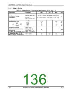
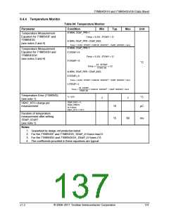
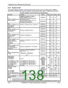
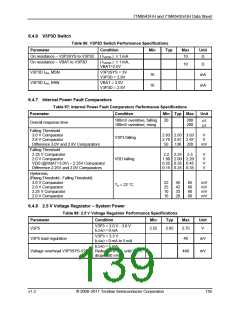
71M6543F/H and 71M6543G/GH Data Sheet
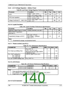
6.4.9 2.5 V Voltage Regulator – Battery Power
Table 99: Low-Power Voltage Regulator Performance Specifications
Parameter
Condition
Min
Typ
Max
Unit
VBAT = 3.0 V - 3.8 V,
V3P3 = 0 V, ILOAD = 0 mA
V2P5
2.55
2.65
2.75
V
VBAT = 3.3 V, V3P3 = 0 V,
ILOAD = 0 mA to 1 mA
V2P5 load regulation
40
mV
mV
ILOAD = 0ma, VBAT = 2.0 V,
V3P3 = 0 V.
Voltage Overhead 2V − VBAT-VDD
200
6.4.10 Crystal Oscillator
Table 100: Crystal Oscillator Performance Specifications
Parameter
Condition
Min
Typ
Max
Unit
Maximum Output Power to Crystal Crystal connected, see note 1
1
μW
XIN to XOUT Capacitance
(see note 1)
3
pF
RTC_ADJ = 7F to 0,
Capacitance change on XOUT
Bias voltage = unbiased
Vpp = 0.1 V
15
pF
Note:
1. Guaranteed by design; not production tested.
6.4.11 Phase-Locked Loop (PLL)
Table 101: PLL Performance Specifications
CONDITION MIN TYP MAX UNIT
PLL_FAST =0,
PARAMETER
V3P3 = 0 to 3.3 V step
Measured from first edge of MCK
(TMUX2OUT pin)
PLL Power-up Settling Time
3
ms
PLL_FAST settling time
PLL_FAST rise
PLL_FAST fall
PLL SLP to MSN Settling Time
V3P3=0, VBAT=3.8 to 2.0 V
3
3
3
ms
ms
ms
PLL_FAST =0
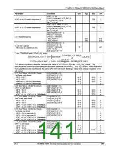
6.4.12 LCD Drivers
Table 102: LCD Drivers Performance Specifications
PARAMETER
VLCD Current
MIN TYP MAX
UNIT
uA
uA
CONDITION
VLCD=3.3, all LCD map bits=0
VLCD=5.0, all LCD map bits=0
2
3
Note:
1. These specifications apply to all COM and SEG pins.
1. LCD_VMODE=3, LCD_ON=1, LCD_BLANK=0, LCD_MODE=6, LCD_CLK=2.
2. Output load is 74 pF per SEG and COM pin.
6.4.13 VLCD Generator
Table 103: VLCD Generator Specifications
140
© 2008–2011 Teridian Semiconductor Corporation
v1.2

 MAXIM [ MAXIM INTEGRATED PRODUCTS ]