SC70, Single/Dual Low-Voltage,
Low-Power µP Reset Circuits
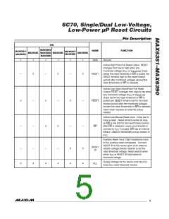
V
V
CC
CC
V
IN
MAX6387
MAX6388
MAX6389
MAX6381
MAX6384
MAX6387
R1
R2
RESET
(RESET)
RESET
RESET IN
R1
100k
GND
GND
( ) IS FOR MAX6388
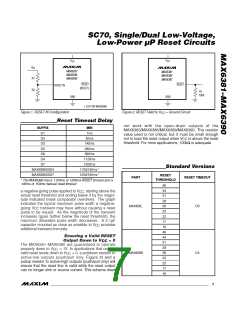
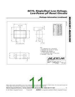
Figure 1. RESET IN Configuration
Figure 2. RESET Valid to V = Ground Circuit
CC
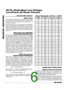
Reset Timeout Delay
not work with the open-drain outputs of the
MAX6383/MAX6386/MAX6389/MAX6390. The resistor
value used is not critical, but it must be small enough
SUFFIX
MIN
D1
1ms
D2
20ms
not to load the reset output when V
is above the reset
CC
threshold. For most applications, 100kΩ is adequate.
D3
140ms
D5
280ms
D6
D4
560ms
1120ms
1200ms
1120/140ms *
1200/150ms *
D7
Standard Versions
MAX6390XSD4
MAX6390XSD7
RESET
THRESHOLD
PART
RESET TIMEOUT
* The MAX6390 has a 1120ms or 1200ms RESET timeout and a
140ms or 150ms manual reset timeout
46
44
31
29
26
23
22
17
16
46
44
31
29
26
23
22
17
16
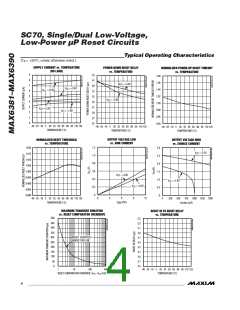
a negative-going pulse applied to V , starting above the
CC
actual reset threshold and ending below it by the magni-
tude indicated (reset comparator overdrive). The graph
indicates the typical maximum pulse width a negative-
MAX638_
D3
going V
transient may have without causing a reset
CC
pulse to be issued. As the magnitude of the transient
increases (goes farther below the reset threshold), the
maximum allowable pulse width decreases. A 0.1µF
capacitor mounted as close as possible to V
additional transient immunity.
provides
CC
Ensuring a Valid RESET
Output Down to V = 0
CC
The MAX6381–MAX6390 are guaranteed to operate
properly down to V = 1V. In applications that require
CC
MAX6390
D4
valid reset levels down to V
= 0, a pulldown resistor to
CC
active-low outputs (push/pull only, Figure 2) and a
pullup resistor to active-high outputs (push/pull only) will
ensure that the reset line is valid while the reset output
can no longer sink or source current. This scheme does
_______________________________________________________________________________________
7

 MAXIM [ MAXIM INTEGRATED PRODUCTS ]