=
=
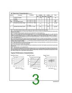
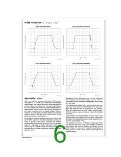
Pulse Response RL 10 kΩ, CL 10 pF
Small Signal Inverting
Small Signal Non-Inverting
DS009156-6
DS009156-7
Large Signal Inverting
Large Signal Non-Inverting
DS009156-8
DS009156-9
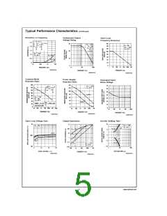
Exceeding the positive common-mode limit on a single input
will not change the phase of the output; however, if both in-
puts exceed the limit, the output of the amplifier will be forced
to a high state.
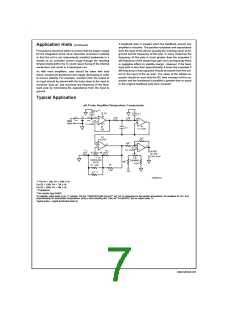
Application Hints
This device is a quad low power op amp with JFET input de-
™
vices ( BI-FET ). These JFETs have large reverse break-
down voltages from gate to source and drain eliminating the
need for clamps across the inputs. Therefore, large differen-
tial input voltages can easily be accommodated without a
large increase in input current. The maximum differential in-
put voltage is independent of the supply voltages. However,
neither of the input voltages should be allowed to exceed the
negative supply as this will cause large currents to flow
which can result in a destroyed unit.
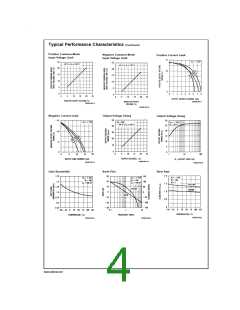
The amplifiers will operate with a common-mode input volt-
age equal to the positive supply; however, the gain band-
width and slew rate may be decreased in this condition.
When the negative common-mode voltage swings to within
3V of the negative supply, an increase in input offset voltage
may occur.
Each amplifier is individually biased to allow normal circuit
±
operation with power supplies of 3.0V. Supply voltages less
Exceeding the negative common-mode limit on either input
will force the output to a high state, potentially causing a re-
versal of phase to the output. Exceeding the negative
common-mode limit on both inputs will force the amplifier
output to a high state. In neither case does a latch occur
since raising the input back within the common-mode range
again puts the input stage and thus the amplifier in a normal
operating mode.
than these may degrade the common-mode rejection and re-
strict the output voltage swing.
±
The amplifiers will drive a 10 kΩ load resistance to 10V
over the full temperature range. If the amplifier is forced to
drive heavier load currents, however, an increase in input
offset voltage may occur on the negative voltage swing and
finally reach an active current limit on both positive and
negative swings.
www.national.com
6

 NSC [ National Semiconductor ]