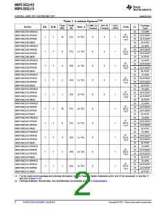
MSP430G2x53
MSP430G2x13
SLAS735A –APRIL 2011–REVISED MAY 2011
www.ti.com
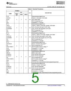
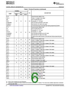
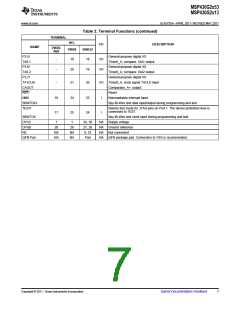
Table 2. Terminal Functions (continued)
TERMINAL
NO.
I/O
DESCRIPTION
NAME
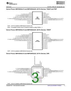
PW20,
N20
PW28
RHB32
P1.6/
General-purpose digital I/O pin
Timer0_A, compare: Out1 output
ADC10 analog input A6(1)
TA0.1/
A6/
CA6/
14
22
21
I/O
Comparator_A+, CA6 input
UCB0SOMI/
UCB0SCL/
TDI/TCLK
P1.7/
USCI_B0 slave out/master in SPI mode,
USCI_B0 SCL I2C clock in I2C mode
JTAG test data input or test clock input during programming and test
General-purpose digital I/O pin
A7/
ADC10 analog input A7(1)
CA7/
Comparator_A+, CA7 input
CAOUT/
UCB0SIMO/
UCB0SDA/
TDO/TDI
Comparator_A+, output
15
23
22
I/O
USCI_B0 slave in/master out in SPI mode
USCI_B0 SDA I2C data in I2C mode
JTAG test data output terminal or test data input during programming and
test(2)
P2.0/
TA1.0
P2.1/
TA1.1
P2.2/
TA1.1
P2.3/
TA1.0
P2.4/
TA1.2
P2.5/
TA1.2
XIN/
General-purpose digital I/O pin
8
10
11
12
16
17
18
9
I/O
I/O
I/O
I/O
I/O
I/O
Timer1_A, capture: CCI0A input, compare: Out0 output
General-purpose digital I/O pin
9
10
11
15
16
17
Timer1_A, capture: CCI1A input, compare: Out1 output
General-purpose digital I/O pin
10
11
12
13
Timer1_A, capture: CCI1B input, compare: Out1 output
General-purpose digital I/O pin
Timer1_A, capture: CCI0B input, compare: Out0 output
General-purpose digital I/O pin
Timer1_A, capture: CCI2A input, compare: Out2 output
General-purpose digital I/O pin
Timer1_A, capture: CCI2B input, compare: Out2 output
Input terminal of crystal oscillator
P2.6/
TA0.1
XOUT/
P2.7
19
27
26
I/O
General-purpose digital I/O pin
Timer0_A, compare: Out1 output
Output terminal of crystal oscillator(3)
18
-
26
9
25
7
I/O
I/O
I/O
I/O
I/O
I/O
General-purpose digital I/O pin
P3.0/
TA0.2
P3.1/
TA1.0
P3.2/
TA1.1
P3.3/
TA1.2
P3.4/
TA0.0
General-purpose digital I/O pin
Timer0_A, capture: CCI2A input, compare: Out2 output
General-purpose digital I/O pin
-
8
6
Timer1_A, compare: Out0 output
General-purpose digital I/O pin
-
13
14
15
12
13
14
Timer1_A, compare: Out1 output
General-purpose digital I/O
-
Timer1_A, compare: Out2 output
General-purpose digital I/O
-
Timer0_A, compare: Out0 output
(2) TDO or TDI is selected via JTAG instruction.
(3) If XOUT/P2.7 is used as an input, excess current will flow until P2SEL.7 is cleared. This is due to the oscillator output driver connection
to this pad after reset.
6
Submit Documentation Feedback
Copyright © 2011, Texas Instruments Incorporated

 TI [ TEXAS INSTRUMENTS ]