MSP430F530x, MSP430F5310
www.ti.com
SLAS677B –SEPTEMBER 2010–REVISED MARCH 2011
Flash Memory
The flash memory can be programmed via the JTAG port, Spy-Bi-Wire (SBW), the BSL, or in-system by the
CPU. The CPU can perform single-byte, single-word, and long-word writes to the flash memory. Features of the
flash memory include:
•
Flash memory has n segments of main memory and four segments of information memory (A to D) of
128 bytes each. Each segment in main memory is 512 bytes in size.
•
•
Segments 0 to n may be erased in one step, or each segment may be individually erased.
Segments A to D can be erased individually, or as a group with segments 0 to n. Segments A to D are also
called information memory.
•
Segment A can be locked separately.
RAM Memory
The RAM memory is made up of n sectors. Each sector can be completely powered down to save leakage,
however all data is lost. Features of the RAM memory include:
•
•
•
RAM memory has n sectors. The size of a sector can be found in the Memory Organization section.
Each sector 0 to n can be completely disabled, however data retention is lost.
Each sector 0 to n automatically enters low power retention mode when possible.
Peripherals
Peripherals are connected to the CPU through data, address, and control buses and can be handled using all
instructions. For complete module descriptions, see the MSP430x5xx/MSP430x6xx Family User's Guide,
literature number SLAU208.
Digital I/O
There are up to six 8-bit I/O ports implemented: For 64 pin options, P1, P2, P4, and P6 are complete, P5 is
reduced to 6-bit I/O, and P3 is reduced to 5-bit I/O. For 48 pin options, P6 is reduced to 4-bit I/O, P2 is reduced
to 1-bit I/O, and P3 is completely removed. Port PJ contains four individual I/O ports, common to all devices.
•
•
•
•
•
•
•
All individual I/O bits are independently programmable.
Any combination of input, output, and interrupt conditions is possible.
Pullup or pulldown on all ports is programmable.
Drive strength on all ports is programmable.
Edge-selectable interrupt and LPM4.5 wakeup input capability is available for all bits of ports P1 and P2.
Read/write access to port-control registers is supported by all instructions.
Ports can be accessed byte-wise (P1 through P6) or word-wise in pairs (PA through PC).
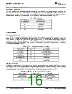
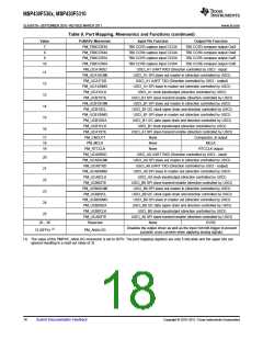
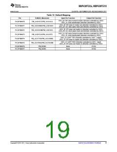
Port Mapping Controller
The port mapping controller allows the flexible and reconfigurable mapping of digital functions to port P4.
Table 9. Port Mapping, Mnemonics and Functions
Value
PxMAPy Mnemonic
PM_NONE
Input Pin Function
Output Pin Function
DVSS
0
None
PM_CBOUT0
PM_TB0CLK
-
Comparator_B output
1
2
TB0 clock input
PM_ADC10CLK
PM_DMAE0
-
ADC10CLK
SVM output
DMAE0 input
-
PM_SVMOUT
3
TB0 high impedance input
TB0OUTH
PM_TB0OUTH
4
5
6
PM_TB0CCR0A
PM_TB0CCR1A
PM_TB0CCR2A
TB0 CCR0 capture input CCI0A
TB0 CCR1 capture input CCI1A
TB0 CCR2 capture input CCI2A
TB0 CCR0 compare output Out0
TB0 CCR1 compare output Out1
TB0 CCR2 compare output Out2
Copyright © 2010–2011, Texas Instruments Incorporated
Submit Documentation Feedback
17

 TI [ TEXAS INSTRUMENTS ]