TMC248-LA DATASHEET (Rev. 1.01 / 2013-MAR-26)
11
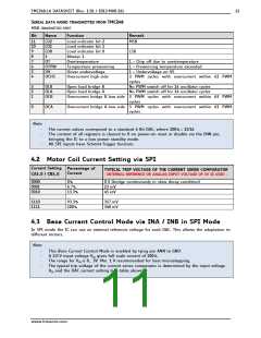
SERIAL DATA WORD TRANSMITTED FROM TMC248
MSB TRANSMITTED FIRST
Bit
Name
Function
Remark
11
10
9
LD2
LD1
LD0
1
Load indicator bit 2
Load indicator bit 1
Load indicator bit 0
Always 1
MSB
LSB
8
7
6
5
4
OT
OTPW
UV
Overtemperature
1 = Chip off due to overtemperature
1 = Prewarning temperature exceeded
1 = Undervoltage on VS
3 PWM cycles with overcurrent within 63 PWM
cycles
Temperature prewarning
Driver undervoltage
Overcurrent high side
OCHS
3
2
1
OLB
OLA
OCB
Open load bridge B
Open load bridge A
No PWM switch off for 14 oscillator cycles
No PWM switch off for 14 oscillator cycles
Overcurrent bridge B low side 3 PWM cycles with overcurrent within 63 PWM
cycles
0
OCA
Overcurrent bridge A low side 3 PWM cycles with overcurrent within 63 PWM
cycles
Note:
-
-
The current values correspond to a standard 4 Bit DAC, where 100% = 15/16.
The content of all registers is cleared to 0 on power-on reset or disable via the ENN pin,
bringing the IC to a low power standby mode.
-
All SPI inputs have Schmitt-Trigger function.
4.2 Motor Coil Current Setting via SPI
Current Setting Percentage of
TYPICAL TRIP VOLTAGE OF THE CURRENT SENSE COMPARATOR
- INTERNAL REFERENCE OR ANALOG INPUT VOLTAGE OF 2V IS USED -
Current
CA3..0 / CB3..0
0000
0001
0010
...
0%
0 V (bridge continuously in slow decay condition)
23 mV
45 mV
6.7%
13.3%
...
1110
1111
93.3%
100%
317 mV
340 mV
4.3 Base Current Control Mode via INA / INB in SPI Mode
In SPI mode the IC can use an external reference voltage for each DAC. This allows the adaptation to
different motors.
Note:
-
-
-
-
This Base Current Control Mode is enabled by tying pin ANN to GND.
A 2.0 V input voltage VIN gives full scale current of 100%.
The range for VIN is 0… 3V. Min. 1 V recommended for best microstepping.
The typical trip voltage of the current sense comparator is determined by the input voltage
VIN and the DAC current setting (see table above).
www.trinamic.com

 TRINAMIC [ TRINAMIC MOTION CONTROL GMBH & CO. KG. ]