TMC6200 DATASHEET (Rev. 1.01 / 2018-NOV-15)
10
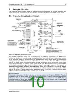
3 Sample Circuits
The following sample circuits show the required external components in different operation and
supply modes. The connection of the bus interface and further digital signals are left out for clarity.
3.1 Standard Application Circuit
+VM
Optional use lower
voltage down to 12V
22n
100V
100n
16V
100n
+VM
CE
470n
VCP
VSA
Use low inductivity SMD
type, e.g. 1210 or 2512
resistor for RS
CB
Gate Voltage
Regulator
12VOUT
Charge Pump
12VOUT
CU
HSU
U
100n
!
4.7µ
2.2µ
HS
LS
RP (optional 10 Ohm to 22
Ohm) protects the sense
amplifier against excessive
spikes on RS
5VOUT
RG
VOFS
5V Regulator
+VIO
IW
3.3V or 5V
I/O voltage
+
USENSE
LSU
RS
VCC_IO
RP
RG
100n
OTP memory
VCP
3 Phase
Motor
opt. ext. Clock 8-33MHz
CLK_IN
UH
CB
24MHz Oscillator
12VOUT
CV
pd
pd
pd
pd
pd
pd
B.Dwersteg, ©
TRINAMIC 2014
HSV
V
HS
LS
UL
RG
VOFS
VH
N
S
Break before
Make logic
IV
VL
+
VSENSE
LSV
RS
RP
RG
WH
WL
VCP
CB
Diagnostics
(Short circuit,
Temperature)
12VOUT
FAULT
CW
5VOUT
Settings in Standalone
mode (SPE=0)
SPI interface
(SPE=1)
HSW
W
HS
LS
Keep inductivity of the fat
interconnections as small as
possible to avoid undershoot
of U/V/W < -5V!
RG
CSN / IDRV0
500k
Driver Strength [IDRV1 IDRV0]:
00: 0.5A 01: 0.5/1A, 10: 1A, 11: 1.5A
SCK / IDRV1
SDI / AMPLx10
SDO / SINGLE
+
WSENSE
LSW
RS
SPI interface
pd
Sense Amplification 0: 5*, 1: 10*
0: xH/xL individual gate control
1: xH=Polarity, xL=Enable control
RP
RG
250k
IU
IV
GND: Stand alone,
VIO: SPI interface mode
Bootstrap capacitors CB:
For MOSFETs with QG<40nC: min. 470nF, 16V
1µF for larger QG - use minimum 4.7µF on 12VOUT pin
Optional slope control resistors RG
:
In case of MOSFETs <20nC, adapt to MOSFET to yield slopes of
roughly 50ns. Slope must be slower than bulk diode recovery time.
1Ohm to 2.2Ohm recommended for larger MOSFETs.
Current Sense
outputs
+VIO
+VIO
Driver Enable
(positive active)
May be left away with compact, low inducivity routing of power stage.
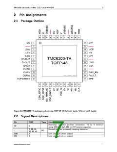
Figure 3.1 Standard application circuit
The standard application circuit uses a minimum set of additional components. Six MOSFETs are
selected for the desired current, voltage and package type. Two or three sense resistors are matched
to the maximum motor coil current, and to the desired current sensor output swing and amplification
setting. See chapter 6.2 to choose the right value for sense resistors. Use low ESR capacitors for
filtering the power supply. A minimum capacity of 100µF per ampere of coil current near to the power
bridge is recommended for keeping power supply ripple low. The capacitors need to cope with the
current ripple caused by chopper operation. Current ripple in the supply capacitors also depends on
the power supply internal resistance and cable length. Supply VCC_IO from 5VOUT, or from an external
source, e.g. a 3.3V regulator. In order to minimize linear voltage regulator power dissipation of the
internal 5V and 11.5V voltage regulators in applications where VM is high, a different (lower) supply
voltage should be used for VSA, when available (see chapter 0).
Basic layout hints
Place sense resistors and all filter capacitors as close as possible to the power MOSFETs. Place the
TMC6200 near to the MOSFETs and use short interconnection lines in order to minimize parasitic trace
inductance. Use a solid common GND for all GND and GNDA connections. Connect 5VOUT filtering
capacitor directly to 5VOUT and GNDA pin. See layout hints for more details. Low ESR electrolytic
capacitors are recommended for VS filtering.
www.trinamic.com

 TRINAMIC [ TRINAMIC MOTION CONTROL GMBH & CO. KG. ]