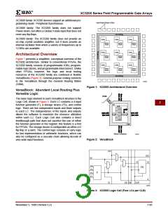
R
XC5200 Series Field Programmable Gate Arrays
tomized RPMs, freeing the designer from the need to
become an expert on architectures.
results or other incoming data in flip-flops, and connect
their outputs to the interconnect network as well. The CLB
storage elements can also be configured as latches.
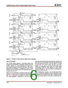
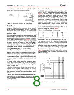
cascade out
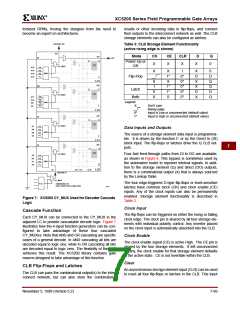
Table 3: CLB Storage Element Functionality
(active rising edge is shown)
CO
DO
Mode
CK
CE
CLR
D
Q
DI
out
Q
D
Power-Up or
GR
X
X
X
X
0
FD
CY_MUX
A15
A14
A13
A12
F4
F3
F2
F1
X
__/
0
X
1*
X
1
X
D
X
X
D
X
0
AND
Flip-Flop
0*
0*
0*
0*
0*
D
Q
Q
D
Q
X
LC3
DO
DI
1
1*
1*
0
Latch
Both
D
Q
0
FD
CY_MUX
A11
A10
A9
F4
F3
F2
F1
X
AND
Legend:
X
X
__/
0*
Don’t care
Rising edge
Input is Low or unconnected (default value)
Input is High or unconnected (default value)
A8
LC2
DO
DI
1*
D
Q
FD
CY_MUX
A7
A6
A5
A4
F4
F3
F2
F1
Data Inputs and Outputs
AND
The source of a storage element data input is programma-
ble. It is driven by the function F, or by the Direct In (DI)
block input. The flip-flops or latches drive the Q CLB out-
puts.
X
LC1
DO
DI
7
Q
D
FD
CY_MUX
Four fast feed-through paths from DI to DO are available,
as shown in Figure 4. This bypass is sometimes used by
the automated router to repower internal signals. In addi-
tion to the storage element (Q) and direct (DO) outputs,
there is a combinatorial output (X) that is always sourced
by the Lookup Table.
A3
A2
A1
A0
F4
F3
F2
F1
AND
X
LC0
CK
CI
CE
CLR
cascade in
CY_MUX
Initialization of
The four edge-triggered D-type flip-flops or level-sensitive
latches have common clock (CK) and clock enable (CE)
inputs. Any of the clock inputs can also be permanently
enabled. Storage element functionality is described in
Table 3.
F=0
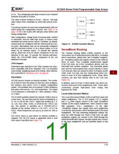
carry chain (One Logic Cell)
X5708
Figure 7: XC5200 CY_MUX Used for Decoder Cascade
Logic
Clock Input
Cascade Function
The flip-flops can be triggered on either the rising or falling
clock edge. The clock pin is shared by all four storage ele-
ments with individual polarity control. Any inverter placed
on the clock input is automatically absorbed into the CLB.
Each CY_MUX can be connected to the CY_MUX in the
adjacent LC to provide cascadable decode logic. Figure 7
illustrates how the 4-input function generators can be con-
figured to take advantage of these four cascaded
CY_MUXes. Note that AND and OR cascading are specific
cases of a general decode. In AND cascading all bits are
decoded equal to logic one, while in OR cascading all bits
are decoded equal to logic zero. The flexibility of the LUT
achieves this result. The XC5200 library contains gate
macros designed to take advantage of this function.
Clock Enable
The clock enable signal (CE) is active High. The CE pin is
shared by the four storage elements. If left unconnected
for any, the clock enable for that storage element defaults
to the active state. CE is not invertible within the CLB.
Clear
CLB Flip-Flops and Latches
An asynchronous storage element input (CLR) can be used
to reset all four flip-flops or latches in the CLB. This input
The CLB can pass the combinatorial output(s) to the inter-
connect network, but can also store the combinatorial
November 5, 1998 (Version 5.2)
7-89

 XILINX [ XILINX, INC ]