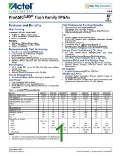
PLUS
ProASIC
Flash Family FPGAs
Device Family Overview
The ProASICPLUS family of devices, Actel’s second-
generation family of flash FPGAs, offers enhanced
performance over Actel’s ProASIC family. It combines the
advantages of ASICs with the benefits of programmable
devices through nonvolatile flash technology. This
enables engineers to create high-density systems using
existing ASIC or FPGA design flows and tools. In addition,
the ProASICPLUS family offers a unique clock conditioning
circuit based on two on-board phase-locked loops (PLLs).
The family offers up to one million system gates,
supported with up to 198 kbits of two-port SRAM and up
to 712 user I/Os, all providing 50 MHz PCI performance.
combination of fine granularity, flexible routing
resources, and abundant flash switches allows 100%
utilization and over 95% routability for highly congested
designs. Tiles and larger functions are interconnected
through a four-level routing hierarchy.
Embedded two-port SRAM blocks with built-in FIFO/RAM
control logic can have user-defined depths and widths.
Users can also select programming for synchronous or
asynchronous operation, as well as parity generations or
checking.
The unique clock conditioning circuitry in each device
includes two clock conditioning blocks. Each block
provides a PLL core, delay lines, phase shifts (0° and
180°), and clock multipliers/dividers, as well as the
circuitry needed to provide bidirectional access to the
PLL. The PLL block contains four programmable
frequency dividers which allow the incoming clock signal
to be divided by a wide range of factors from 1 to 64.
The clock conditioning circuit also delays or advances the
incoming reference clock up to 8 ns (in increments of
0.25 ns). The PLL can be configured internally or
externally during operation without redesigning or
reprogramming the part. In addition to the PLL, there
are two LVPECL differential input pairs to accommodate
high-speed clock and data inputs.
Advantages
to
the
designer
extend
beyond
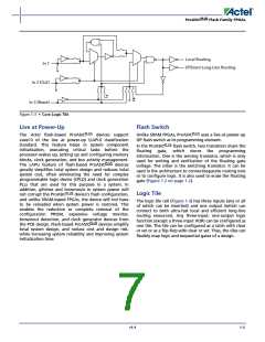
performance. Unlike SRAM-based FPGAs, four levels of
routing hierarchy simplify routing, while the use of flash
technology allows all functionality to be live at power-
up. No external boot PROM is required to support device
programming. While on-board security mechanisms
prevent
access
to
the
program
information,
reprogramming can be performed in-system to support
future design iterations and field upgrades. The device’s
architecture mitigates the complexity of ASIC migration
at higher user volume. This makes ProASICPLUS a cost-
effective solution for applications in the networking,
communications, computing, and avionics markets.
The ProASICPLUS family achieves its nonvolatility and
reprogrammability through an advanced flash-based
0.22 μm LVCMOS process with four layers of metal.
Standard CMOS design techniques are used to
implement logic and control functions, including the
PLLs and LVPECL inputs. This results in predictable
performance compatible with gate arrays.
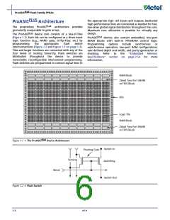
The ProASICPLUS architecture provides granularity
comparable to gate arrays. The device core consists of a
Sea-of-Tiles™. Each tile can be configured as a flip-flop,
latch, or three-input/one-output logic function by
programming the appropriate Flash switches. The
To support customer needs for more comprehensive,
lower-cost, board-level testing, Actel’s ProASICPLUS
devices are fully compatible with IEEE Standard 1149.1
for test access port and boundary-scan test architecture.
For more information concerning the flash FPGA
implementation, please refer to the "Boundary Scan
(JTAG)" section on page 2-8.
ProASICPLUS devices are available in a variety of high-
performance plastic packages. Those packages and the
performance features discussed above are described in
more detail in the following sections.
v5.9
1-1

 ACTEL [ Actel Corporation ]