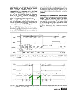
External DATACLK Active After the Conversion
and During the Next Conversion
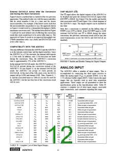
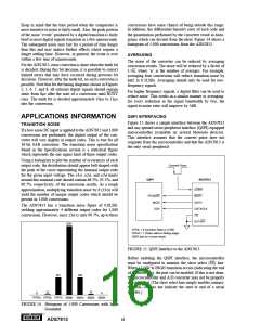
CHIP SELECT (CS)
The CS input allows the digital outputs of the ADS7812 to
be disabled and gates the external DATACLK signal when
EXT/INT is HIGH. See Figure 9 for the enable and disable
time associated with CS and Figure 3 for a block diagram of
the ADS7813’s logic. The digital outputs can be disabled at
any time.
Figure 8 shows a method that is a hybrid of the two previous
approaches. This method works very well for microcontrollers
that do serial transfers 8 bits at a time and for slower
microcontrollers. For example, if the fastest serial clock that
the microcontroller can produce is 1µs, the approach shown
in Figure 6 would result in a diminished throughput (26kHz
maximum conversion rate). The method described in Figure
7 could not be used without risk of affecting the conversion
result (the clock would have to be active after time t2). The
approach in Figure 8 results in an improved throughput rate
(33kHz maximum with a 1µs clock) and DATACLK is not
active after time t2.
Note that a conversion is initiated on the falling edge of
CONV even if CS is HIGH. If the EXT/INT input is LOW
(internal DATACLK) and CS is HIGH during the entire
conversion, the previous conversion result will be lost (the
serial transmission occurs but DATA and DATACLK are
disabled).
CS
COMPATIBILITY WITH THE ADS7812
The only difference between the ADS7812 and the ADS7813
is in the internal control logic and the digital interface. Since
the ADS7812 is a 12-bit converter, the internal shift register
is 12 bits wide. In addition, only 12-bit decisions are made
during the conversion. Thus, the ADS7812’s conversion
time is approximately 75% of the ADS7813’s.
t26
t27
BUSY, DATA,
DATACLK(1)
HI-Z
Active
HI-Z
NOTE: (1) DATACLK is an output only when EXT/INT is LOW.
FIGURE 9. Enable and Disable Timing for Digital Outputs.
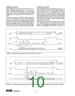
In the internal DATACLK mode, the ADS7812 produces 12
DATACLK periods during the conversion instead of the
ADS7813’s 16 (see Figure 5). In the external DATACLK
mode, the ADS7812 can accept 16 clock periods on
DATACLK. At the start of the 13th clock cycle, the DATA
output will go LOW and remain LOW. Thus, Figures 6, 7,
8, and the associated times in Table II can also be used for
the ADS7812, but the last four bits of the conversion result
will be zero.
ANALOG INPUT
The ADS7813 offers a number of input ranges. This is
accomplished by connecting the three input resistors to
either the analog input (VIN), to ground (GND), or to the
2.5V reference buffer output (BUF). Table I shows the input
ranges that are typically used in most data acquisition
applications. These ranges are all guaranteed to meet the
specifications given in the Specifications table. Table IV
contains a complete list of ideal input ranges, associated
input connections, and comments regarding the range.
ANALOG
INPUT
RANGE (V)
CONNECT
R1IN
CONNECT
R2IN
CONNECT
R3IN
TO
INPUT
IMPEDANCE
(kΩ)
TO
TO
COMMENT
0.3125 to 2.8125
–0.417 to 2.916
0.417 to 3.750
±3.333
VIN
VIN
VIN
VIN
VIN
BUF
GND
VIN
> 10,000
26.7
26.7
21.3
45.7
45.7
21.3
45.7
45.7
45.7
21.3
21.3
26.7
26.7
45.7
21.3
21.3
26.7
26.7
Guaranteed offset and gain
VIN cannot go below GND – 0.3V
Offset and gain not guaranteed
Guaranteed offset and gain
VIN
VIN
VIN
BUF
BUF
BUF
GND
GND
GND
VIN
–15 to 5
VIN
BUF
GND
VIN
Offset and gain not guaranteed
Guaranteed offset and gain
±10
VIN
0.833 to 7.5
–2.5 to 17.5
2.5 to 22.5
0 to 2.857
–1 to 3
VIN
Offset and gain not guaranteed
Exceeds absolute maximum VIN
Exceeds absolute maximum VIN
Offset and gain not guaranteed
VIN cannot go below GND – 0.3V
Guaranteed offset and gain
VIN
BUF
GND
VIN
VIN
BUF
BUF
BUF
BUF
BUF
GND
GND
GND
GND
GND
VIN
BUF
GND
VIN
0 to 4
VIN
–6.25 to 3.75
0 to 10
BUF
GND
VIN
Offset and gain not guaranteed
Guaranteed offset and gain
VIN
0.357 to 3.214
–0.5 to 3.5
0.5 to 4.5
±5
VIN
Offset and gain not guaranteed
VIN cannot go below GND – 0.3V
Guaranteed offset and gain
VIN
BUF
GND
VIN
VIN
BUF
GND
Guaranteed offset and gain
1.25 to 11.25
VIN
Offset and gain not guaranteed
TABLE IV. Complete List of Ideal Input Ranges.
®
ADS7813
12

 BB [ BURR-BROWN CORPORATION ]