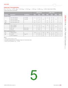
Data Sheet
therefore makes the part easier to drive than previous
flash converters. The preamplifiers also add a gain of two
to the input signal so that each comparator has a wider
overdrive or threshold range to “trip” into or out of the
active state. This gain reduces metastable states that can
cause errors at the output.
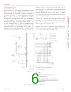
General Description
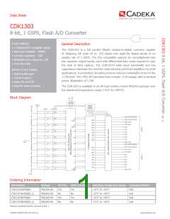
The CDK1303 is one of the fastest monolithic 8-bit parallel
flash A/D converters available today. The nominal
conversion rate is 1 GSPS and the analog bandwidth is
in excess of 900MHz. A major advance over previous
flash converters is the inclusion of 256 input preamplifiers
between the reference ladder and input comparators
(see block diagram). This not only reduces clock transient
kickback to the input and reference ladder due to a low
AC beta, but also reduces the effect of the dynamic state
of the input signal on the latching characteristics of the
input comparators. The preamplifiers act as buffers and
stabilize the input capacitance so that it remains constant
over different input voltage and frequency ranges and
The CDK1303 has true differential analog and digital
data paths from the preamplifiers to the output buffers
(Current Mode Logic) for reducing potential missing codes
while rejecting common mode noise.
Signature errors are also reduced by careful layout of the
analog circuitry. The output drive capability of the device
can provide full ECL swings into 50Ω loads.
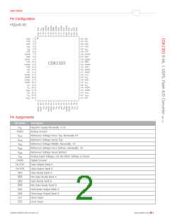
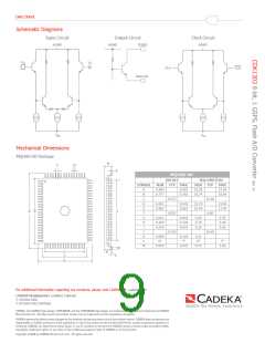
Figure 1. Typical Interface Circuit Diagram
©2008 CADEKA Microcircuits LLC
www.cadeka.com
6

 CADEKA [ CADEKA MICROCIRCUITS LLC. ]