Data Sheet
to the state prior to the clock transition and output logic
codes in sequence from the top comparators, closest to
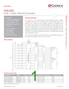
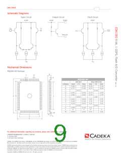
Operation
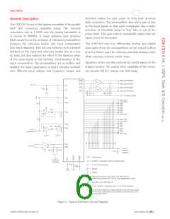
The CDK1303 has 256 preamp/comparator pairs which are
V
(0V), down to the point where the magnitude of the
RT
each supplied with the voltage from V to V divided
RT
RB
input signal changes sign (thermometer code). The output
of each comparator is then registered into four 64-to-6
bit decoders when the CLK is changed from high to low.
At the output of the decoders is a set of four 7-bit latches
which are enabled (“track”) when the clock changes from
high to low. From here, the output of the latches are
coded into 6 LSBs from 4 columns and 4 columns are coded
into 2 MSBs. Finally, 8 ECL output latches and buffers
are used to drive the external loads. The conversion
takes one clock cycle from the input to the data outputs.
equally by the resistive ladder as shown in the block
diagram. This voltage is applied to the positive input of
each preamplifier/comparator pair. An analog input volt-
age applied at V is connected to the negative inputs of
IN
each preamplifier/comparator pair. The comparators are
then clocked through each one’s individual clock buffer.
When the CLK pin is in the low state, the master or input
stage of the comparators compare the analog input volt-
age to the respective reference voltage. When the CLK
pin changes from low to high the comparators are latched
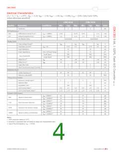
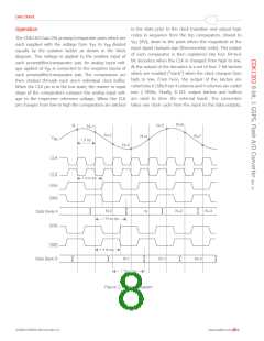
N+6
N
N+5
N+1
N+2
N+4
N+7
V
IN
1.0 ns
N+3
CLK
CLK
DRA
1.4 ns typ
DRA
N-2
N+2
N+4
N
Data Bank A
1.75 ns typ
DRB
DRB
1.4 ns typ
Data Bank B
N-1
N+1
N+3
1.75 ns typ
Figure 2. Timing Diagram
©2008 CADEKA Microcircuits LLC
www.cadeka.com
8

 CADEKA [ CADEKA MICROCIRCUITS LLC. ]