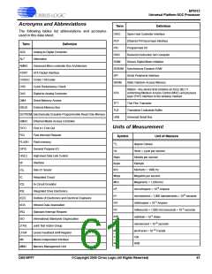
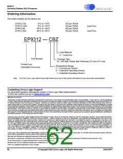
EP9312
Universal Platform SOC Processor
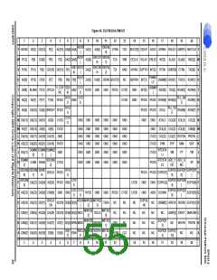
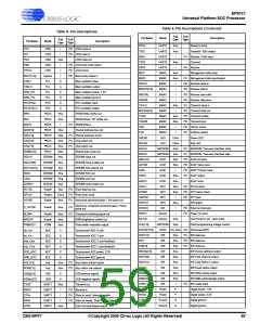
The following section focuses on the EP9312 pin signals
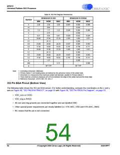
Under the Pad Type column:
from two viewpoints
- the pin usage and pad
•
•
•
•
•
•
•
•
A - Analog pad
characteristics, and the pin multiplexing usage. The first
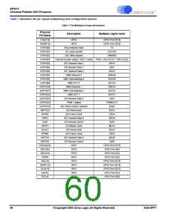
table (Table S) is a summary of all the EP9312 pin
signals. The second table (Table T) illustrates the pin
signal multiplexing and configuration options.
P - Power pad
G - Ground pad
I - Pin is an input only
I/O - Pin is input/output
4mA - Pin is a 4 mA output driver
8mA - Pin is an 8 mA output driver
12mA - Pin is an 12 mA output driver
Table S is a summary of the EP9312 pin signals, which
illustrates the pad type and pad pull type (if any). The
symbols used in the table are defined as follows. (Note: A
blank box means Not Applicable (NA) or, for Pull Type,
No Pull (NP).)
See the text description for additional information about
bi-directional pins.
Under the Pull Type Column:
•
•
PU - Resistor is a pull up to the RVDD supply
PD - Resistor is a pull down to the RGND supply
58
©Copyright 2005 Cirrus Logic (All Rights Reserved)
DS515PP7

 CIRRUS [ CIRRUS LOGIC ]