Power Characteristics
1,2
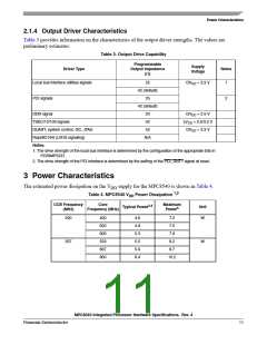
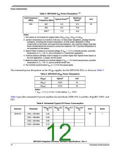
Table 4. MPC8540 V Power Dissipation
DD
CCB Frequency
Core
Frequency (MHz)
Maximum
Power5
Typical Power3,4
Unit
(MHz)
333
667
833
6.3
6.9
9.3
W
10.9
15.9
1000 6
11.3
Notes:
1. The values do not include I/O supply power (OVDD, LVDD, GVDD) or AVDD
.
2. Junction temperature is a function of die size, on-chip power dissipation, package thermal
resistance, mounting site (board) temperature, air flow, power dissipation of other
components on the board, and board thermal resistance. Any customer design must take
these considerations into account to ensure the maximum 105 °C junction temperature is
not exceeded on this device.
3. Typical Power is based on a nominal voltage of VDD = 1.2 V, a nominal process, a junction
temperature of Tj = 105 °C, and a Dhrystone 2.1 benchmark application.
4. Thermal solutions will likely need to design to a number higher than Typical Power based on
the end application, TA target, and I/O power.
5. Maximum power is based on a nominal voltage of VDD = 1.2 V, worst case process, a junction
temperature of Tj = 105 °C, and an artificial smoke test.
6. The nominal recommended VDD is 1.3 V for this speed grade.
The estimated power dissipation on the AV supplies for the MPC8540 PLLs is shown in Table 5.
DD
Table 5. MPC8540 AV Power Dissipation
DD
AVDD
n
Typical1
Unit
AVDD
1
2
0.007
0.014
W
W
AVDD
Notes:
1. VDD = 1.2 V (1.3 V for 1.0 GHz device), TJ = 105°C
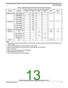
Table 6 provides estimated I/O power numbers for each block: DDR, PCI, Local Bus, RapidIO, TSEC, and
FEC.
Table 6. Estimated Typical I/O Power Consumption
GVDD (2.5 OVDD (3.3
LVDD (3.3
V)
LVDD (2.5
V)
Interface
Parameter
Units
Notes
V)
V)
DDR I/O
CCB = 200 MHz
CCB = 266 MHz
CCB = 300 MHz
CCB = 333 MHz
0.46
0.59
0.66
0.73
W
1
MPC8540 Integrated Processor Hardware Specifications, Rev. 4
12
Freescale Semiconductor

 FREESCALE [ Freescale ]