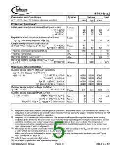
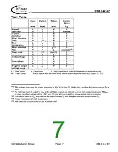
BTS 640 S2
Parameter and Conditions
Symbol
Values
Unit
at Tj = 25 °C, V = 12 V unless otherwise specified
bb
min
typ
max
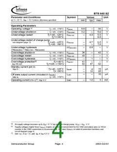
Protection Functions8)
Initial peak short circuit current limit (pin 4 to 6&7)
IL(SCp)
Tj =-40°C:
48
40
31
56
50
37
65
58
45
A
Tj =25°C:
Tj =+150°C:
Repetitive short circuit shutdown current limit
IL(SCr)
T = T (see timing diagrams, page 12)
jt
--
24
--
A
V
j
Output clamp (inductive load switch off)
at V = V - V ; I = 40 mA,
T =-40°C: VON(CL)
41
43
--
47
--
52
OUT bb ON(CL) L
j
Tj =+25..+150°C:
Thermal overload trip temperature
Thermal hysteresis
Tjt
150
--
--
10
--
--
--
°C
K
∆Tjt
-Vbb
9)
Reverse battery (pin 4 to 2)
--
32
V
Reverse battery voltage drop (V
L
> V )
bb
out
I = -5 A
T=150 °C: -VON(rev)
--
600
--
mV
j
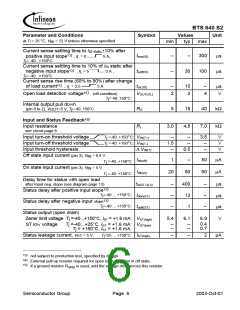
Diagnostic Characteristics
Current sense ratio10), static on-condition,
11)
= 6.5 ...27V,
bb(on)
V
k
= 0...5 V, V
= I / I
IS
Tj = -40°C, IL = 5 A:
kILIS
4550 5000 6000
3300 5000 8000
ILIS
L
IS
Tj= -40°C, IL= 0.5 A:
Tj= 25...+150°C, IL= 5 A:
Tj= 25...+150°C, IL = 0.5 A:
4550 5000 5550
4000 5000 6500
,
Current sense output voltage limitation
T = -40 ...+150°C
I
= 0, I = 5 A:
j
IS L
VIS(lim)
5.4
6.1
6.9
V
Current sense leakage/offset current
T = -40 ...+150°C
V =0, V = 0, I = 0:
j
IN IS
L
IIS(LL)
IIS(LH)
IIS(SH)
0
0
0
--
--
--
1
15
10
µA
V =5 V, V = 0, I = 0:
IN IS
L
12 )
V =5 V, V = 0, V
IN IS
= 0 (short circuit):
OUT
8)
9)
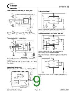
Integrated protection functions are designed to prevent IC destruction under fault conditions described in the
data sheet. Fault conditions are considered as "outside" normal operating range. Protection functions are not
designed for continuous repetitive operation.
Requires 150 Ω resistor in GND connection. The reverse load current through the intrinsic drain-source
diode has to be limited by the connected load. Note that the power dissipation is higher compared to normal
operating conditions due to the voltage drop across the intrinsic drain-source diode. The temperature
protection is not active during reverse current operation! Input and Status currents have to be limited (see
max. ratings page 2 and circuit page 9).
10)
This range for the current sense ratio refers to all devices. The accuracy of the kILIS can be raised at least by
a factor of two by matching the value of kILIS for every single device.
In the case of current limitation the sense current IIS is zero and the diagnostic feedback potential VST is
High. See figure 2b, page 11.
11)
12)
Valid if Vbb(u rst) was exceeded before.
not subject to production test, specified by design
Semiconductor Group
Page 5
2003-Oct-01

 INFINEON [ Infineon ]