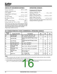
ABSOLUTE MAXIMUM RATINGS
OPERATING RANGES
Storage Temperature . . . . . . . . . . . . . .-65°C to +150°C
Commercial (C) Devices
Ambient Temperature with
Power Applied . . . . . . . . . . . . . . . . . .-55°C to +125°C
Ambient Temperature (T )
A
Operating in Free Air . . . . . . . . . . . . . . . 0°C to +75°C
Supply Voltage with Respect
to Ground . . . . . . . . . . . . . . . . . . . . . -0.5 V to +7.0 V
Supply Voltage (V ) with
CC
Respect to Ground. . . . . . . . . . . . . +4.75 V to +5.25 V
DC Input Voltage . . . . . . . . . . . .-0.5 V to V + 1.0 V
CC
Operating ranges define those limits between which the func-
tionality of the device is guaranteed.
DC Output or I/O Pin Voltage . . .-0.5 V to V + 1.0 V
CC
Static Discharge Voltage . . . . . . . . . . . . . . . . . 2001 V
Latchup Current (T = 0°C to +75°C) . . . . . . . . 100 mA
A
Stresses above those listed under Absolute Maximum Ratings
may cause permanent device failure. Functionality at or above
these limits is not implied. Exposure to absolute maximum rat-
ings for extended periods may affect device reliability.
Programming conditions may vary.
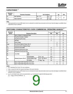
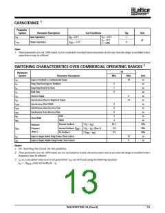
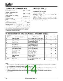
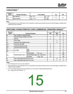
DC CHARACTERISTICS OVER COMMERCIAL OPERATING RANGES
Parameter
Symbol
Parameter Description
Output HIGH Voltage
Output LOW Voltage
Test Conditions
Min
Max
Unit
V
V
I
= -3.2 mA, V = V or V V = Min
IN IH IL, CC
2.4
OH
OH
V
I
= 16 mA, V = V or V V = Min
0.4
V
OL
OL
IN IH
IL, CC
V
Input HIGH Voltage
Guaranteed Input Logical HIGH Voltage for all Inputs (Note 1)
2.0
V
IH
Guaranteed Input Logical LOW
Voltage for all Inputs (Note 1)
V
Input LOW Voltage
0.8
V
IL
I
Input HIGH Leakage Current
Input LOW Leakage Current
V = V , V = Max (Note 2)
IN CC CC
10
µA
µA
IH
I
V = 0 V, V = Max (Note 2)
-100
IL
IN
CC
Off-State Output Leakage
Current HIGH
I
V
= V , V = Max, V = V or V (Note 2)
10
µA
µA
OZH
OUT CC CC
IN IL IH
Off-State Output Leakage
Current LOW
V
= 0 V, V = Max
CC
OUT
I
-100
OZL
V = V or V (Note 2)
IN IL IH
Output Short-Circuit
Current
V
= 0.5 V, VCC = Max
OUT
I
-30
-130
120
mA
mA
SC
T = 25°C (Note 3)
A
I
(Dynamic)
Supply Current
Outputs Open , (I
= 0 mA), V = Max, f = 25 MHz
CC
OUT
CC
Notes:
1. These are absolute values with respect to the device ground, and all overshoots due to system and tester noise are included.
2. I/O pin leakage is the worst case of I and I (or I and I ).
IL OZL IH OZH
3. Not more than one output should be tested at a time. Duration of the short-circuit test should not exceed one second.
V
= 0.5 V has been chosen to avoid test problems caused by tester ground degradation.
OUT
12
PALCE22V10H-10 (Com’l)

 LATTICE [ LATTICE SEMICONDUCTOR ]