LT3592
APPLICATIONS INFORMATION
As the input voltage increases, the inductor current ramps
up more quickly, the number of skipped pulses increases,
and the output voltage ripple increases. For operation
Characteristics section of this data sheet that show the
maximum load current as a function of input voltage and
inductor value for several popular output voltages. Low
inductance may result in discontinuous mode operation,
which is acceptable, but further reduces maximum load
current. For details of the maximum output current and
discontinuous mode operation, see Linear Technology
Application Note 44.
above V
, the only component requirement is that
IN(MAX)
they be adequately rated for operation at the intended
voltage levels.
The LT3592 is robust enough to survive prolonged opera-
tion under these conditions as long as the peak inductor
current does not exceed 1.2A. Inductor saturation due to
high current may further limit performance in this operat-
ing regime.
Catch Diode
Depending on load current, a 500mA to 1A Schottky di-
ode is recommended for the catch diode, D1. The diode
must have a reverse voltage rating equal to or greater
than the maximum input voltage. The ON Semiconductor
MBRA140T3andCentralSemiconductorCMMSH1-40are
good choices, as they are rated for 1A continuous forward
current and a maximum reverse voltage of 40V.
Inductor Selection and Maximum Output Current
A good first choice for the inductor value is:
V
OUT + 0.2V + VD
(
)
L =1.2A •
ƒ
Input Filter Network
where V is the forward voltage drop of the catch diode
D
(~0.4V), f is the switching frequency in MHz and L is in μH.
Withthisvalue,therewillbenosubharmonicoscillationfor
applications with 50% or greater duty cycle. For low duty
For applications that only require a capacitor, bypass V
IN
with a 1μF or higher ceramic capacitor of X7R or X5R
type. Y5V types have poor performance over tempera-
ture and applied voltage and should not be used. A 1μF
ceramic capacitor is adequate to bypass the LT3592 and
will easily handle the ripple current. However, if the input
power source has high impedance, or there is significant
inductance due to long wires or cables, additional bulk
capacitance might be necessary. The can be provided
with a low performance (high ESR) electrolytic capacitor
in parallel with the ceramic device.
cycle applications in which V is more than three times
IN
V
, a good guide for the minimum inductor value is
OUT
ꢁ
ꢄ ꢁ
ꢄ
V ꢀ V ꢀ 0.2V
VOUT + 0.2V + VD
(
)
(
)
IN
OUT
L =1.7 •
•
ꢃ
ꢆ ꢃ
ꢆ
V ꢀ VSW + VD
ƒ
ꢂ
ꢅ ꢂ
ꢅ
IN
where V
is the switch voltage drop (about 0.3V at
SW
500mA).Theinductor’sRMScurrentratingmustbegreater
thanyourmaximumloadcurrentanditssaturationcurrent
should be about 30% higher. For robust operation in fault
conditions,thesaturationcurrentshouldbeabove1.5A.To
keepefficiencyhigh,theseriesresistance(DCR)shouldbe
less than 0.1ꢀ. Table 2 lists several inductor vendors.
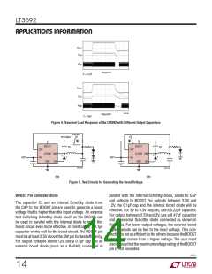
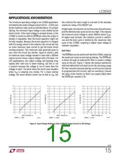
Some applications, such as those in automobiles, may
require extra filtering due to EMI/EMC requirements. In
these applications, very effective EMI filtering can be pro-
vided by a capacitor to ground right at the source voltage,
aseriesferritebead, andapifiltercomposedofacapacitor
toground, aseriesinductor, andanothercapacitordirectly
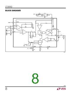
from the device pin to ground (see the Block Diagram for
an example). Typical values for the filter components are
10nF for C2C, a ferrite bead that is ~220ꢀ at 100MHz for
L2, 3.3μF for C2B, 10μH for L3, and 1μF for C2A.
Of course, such a simple design guide will not always re-
sult in the optimum inductor for your application. A larger
valueprovidesahighermaximumloadcurrentandreduces
output voltage ripple at the expense of a slower transient
response. If your load is lower than 500mA, then you can
decrease the value of the inductor and operate with higher
ripple current. This allows you to use a physically smaller
inductor, or one with a lower DCR resulting in higher effi-
ciency.ThereareseveralgraphsintheTypicalPerformance
Step-down regulators draw current from the input sup-
ply in pulses with very fast rise and fall times. The input
capacitor is required to reduce the resulting voltage ripple
3592fc
12

 Linear Systems [ Linear Systems ]