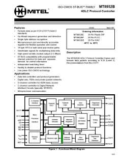
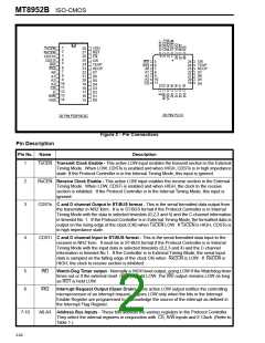
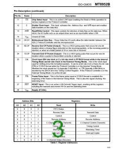
MT8952B ISO-CMOS
address detection can be limited only to the upper
six bits by setting HIGH both RA6/7 and RxAD bits in
the Control Register.
Introduction
The MT8952B HDLC Protocol Controller handles bit
oriented protocol structure and formats the data as
per the packet switching protocol defined in the X.25
Frame Check Sequence (FCS):
(Level 2) recommendations of the CCITT.
It
transmits and receives the packeted data
(information or control) serially in a format shown in
Figure 3 , while providing the data transparency by
zero insertion and deletion. It generates and detects
the flags, various link channel states and the abort
sequence. Further, it provides a cyclic redundancy
check on the data packets using the CCITT defined
polynomial. In addition, it can generate and detect a
Go Ahead sequence and recognize a single byte
address in the received frame. There is also a
provision to disable the protocol functions and
provide transparent access to the serial bus through
the parallel port.
The 16 bits following the data field are the frame
check sequence bits. The generator polynomial is:
16 12
5
G(x)=x +x +x +1
The transmitter calculates the FCS on all bits of the
data field and transmits after the data field and
before the end flag. The receiver performs a similar
computation on all bits of the received data and FCS
fields and the result is compared with FOB8 . If it
Hex
matches, the received data is assumed error free.
The error status of the received packet is indicated
by D7 and D6 bits in the FIFO Status Register.
Zero Insertion and Deletion:
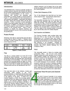
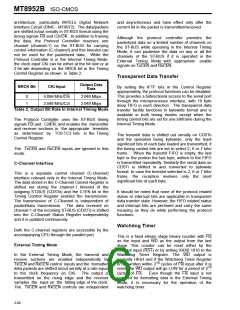
Frame Format
The Protocol Controller, while sending either data
from the FIFO or the 16 bits FCS, checks the
transmission on a bit-by-bit basis and inserts a
ZERO after every sequence of five contiguous ONEs
(including the last five bits of FCS) to ensure that the
All frames start with an opening flag and end with a
closing flag as shown in Figure 3. Between these
two flags, a frame contains the data and the frame
check sequence (FCS).
flag sequence is not simulated.
Similarly the
receiver examines the incoming frame content and
discards any ZERO directly following the five
contiguous ONEs.
FLAG
DATA FIELD
FCS
FLAG
One
Byte
n Bytes
(n ≥ 2)
Two
Bytes
One
Byte
Abort:
Figure 3. Frame Format
The transmitter aborts a frame by sending eight
Flag:
consecutive ONEs.
The FA bit in the Control
Register along with a write operation to the Transmit
Data Register enables the transmission of abort
sequence instead of the byte written to the register.
On the receive side, the ABRT bit in the General
Status Register is set whenever an abort sequence
(7 or more continuous 1’s) is received. The abort
sequence causes the receiver to abandon whatever
it was doing and start searching for a start flag. The
FA bit in the Interrupt Status Register is set when an
abort sequence is received following a start flag and
at least four data bytes (minimum for a valid frame).
The flag is a unique pattern of 8 bits (01111110)
defining the frame boundary. The transmit section
generates the flags and appends them automatically
to the frame to be transmitted. The receive section
searches the incoming packets for flags on a bit-by-
bit basis and establishes frame synchronization. The
flags are used only to identify and synchronize the
received frame and are not transferred to the FIFO.
Data:
The data field refers to the Address, Control and
Interframe Time Fill and Link Channel
States
Information
fields
defined
in
the
CCITT
recommendations. A valid frame should have a data
field of at least 16 bits. The first byte in the data field
is the address of the frame. If RxAD bit in the
Control Register is HIGH, the incoming packet is
recognized only if the address byte matches the byte
stored in the Receive Address Register or the
address byte is the All-Call Address (all ONEs). The
LSB of the Receive Address Register is set LOW
permanently and the comparison is done only on
upper seven bits of the received address byte. The
When the HDLC Protocol Controller is not sending
packets, the transmitter can be in any of three states
mentioned below depending on the status of the
IFTF0 and IFTF1 bits in the Control Register. These
bits are also used to disable the protocol function to
provide the transparent parallel access to the serial
bus through the microprocessor port.
3-64

 MITEL [ MITEL NETWORKS CORPORATION ]