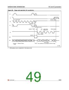
NAND01G-B2B, NAND02G-B2C
DC and AC parameters
(1)
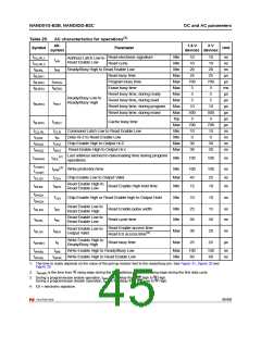
Table 25. AC characteristics for operations
Alt.
1.8 V
devices devices
3 V
Symbol
Parameter
Unit
symbol
tALLRL1
tALLRL2
tBHRL
Read electronic signature
Read cycle
Min
Min
10
10
20
25
700
3
10
10
20
25
700
3
ns
ns
ns
µs
µs
ms
µs
µs
µs
µs
µs
µs
ns
ns
ns
ns
Address Latch Low to
Read Enable Low
tAR
tRR
Ready/Busy High to Read Enable Low
Read busy time
Min
tBLBH1
tBLBH2
tBLBH3
Max
Max
Max
Max
Max
Max
Max
Typ
tPROG
tBERS
Program busy time
Erase busy time
Reset busy time, during ready
5
5
Ready/Busy Low to
Ready/Busy High
Reset busy time, during read
Reset busy time, during program
Reset busy time, during erase
5
5
tBLBH4
tRST
10
500
3
10
500
3
tBLBH5
tCBSY
Cache busy time
Max
Min
700
10
0
700
10
0
tCLLRL
tDZRL
tEHQZ
tRHQZ
tCLR
tIR
tCHZ
tRHZ
Command Latch Low to Read Enable Low
Data Hi-Z to Read Enable Low
Min
Chip Enable High to Output Hi-Z
Read Enable High to Output Hi-z
Max
Max
30
30
30
30
Last address latched to data loading time during program
operations
(2)
tWHWH
tADL
Min
100
100
ns
tVHWH
tVLWH
tELQV
(3)
tWW
Write protection time
Min
Max
Min
100
45
100
25
ns
ns
ns
tCEA
tREH
Chip Enable Low to Output Valid
Read Enable High to
Read Enable High hold time
Read Enable Low
tRHRL
15
10
tEHQX
tRHQX
TOH
Chip Enable High or Read Enable high to Output Hold
Min
10
10
ns
Read Enable Low to
Read Enable pulse width
Read Enable High
tRLRH
tRLRL
tRP
tRC
Min
Min
25
50
15
30
ns
ns
Read Enable Low to
Read cycle time
Read Enable Low
Read Enable access time
Read ES access time(4)
Read Enable Low to
Output Valid
tRLQV
tREA
Max
Max
30
25
20
25
ns
µs
Write Enable High to
Ready/Busy High
tWHBH
tR
Read busy time
tWHBL
tWHRL
tWB
Write Enable High to Ready/Busy Low
Write Enable High to Read Enable Low
Max
Min
100
60
100
60
ns
ns
tWHR
1. The time to ready depends on the value of the pull-up resistor tied to the ready/busy pin. See Figure 31, Figure 32 and
Figure 33.
2. tWHWH is the time from W rising edge during the final address cycle to W rising edge during the first data cycle.
3. During a program/erase enable operation, tWW is the delay from WP high to W High.
During a program/erase disable Operation, tWW is the delay from WP Low to W High.
4. ES = electronic signature.
45/60

 NUMONYX [ NUMONYX B.V ]