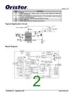
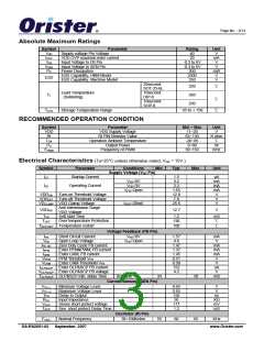
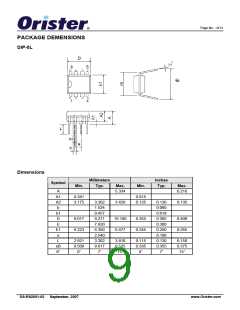
Page No. : 4/13
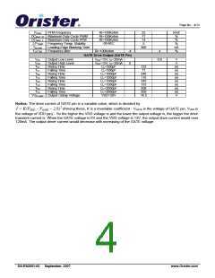
FPFM
PFM Frequency
RI=100Kohm
RI=100Kohm
RI=100Kohm
-30-85℃
22
77
14
5
KHZ
%
%
%
nS
%
DCMAX_W Maximum Duty Cycle PWM
DCMAX_F Maximum Duty Cycle PFM
ΔFTEMP
TBLANK
FJITTER
Frequency Temp. Stability
Leading-Edge Blanking Time
Frequency jitter
300
RI=100Kohm
-4
4
GATE Drive Output (GATE Pin)
VOL
VOH
TR1
TF1
TR2
TF2
TR3
TF3
TR4
TF4
Output Low Level
Output High Level
Rising Time
Falling Time
Rising Time
Falling Time
Rising Time
Falling Time
Rising Time
VDD=15V, IO=20mA
VDD=15V, IO=20mA
CL=500pF
0.8
V
V
9
123
71
ns
ns
ns
ns
ns
ns
ns
ns
V
CL=500pF
CL=1000pF
CL=1000pF
CL=1500pF
CL=1500pF
CL=2000pF
CL=2000pF
VDD=20V
248
116
343
153
508
209
16.5
Falling Time
VGCLAMP Output Clamp Voltage
Notice: The drive current of GATE pin is a variable value, which is decided by
I = K(VVDD −VGATE − 2.8)2 (Among these, K is a invariable coefficient,VGATE is the voltage of GATE pin, VVDD is
the voltage of VDD pin);So the higher the VDD voltage is and the lower the output voltage is, the bigger the drive
transient current is. When the GATE voltage is 0V and the VDD voltage is 13V, the output drive current would over
120mA. The output driver current would decrease with increasing of the GATE voltage.
DS-RS2051-02
September, 2007
www.Orister.com

 ORISTER [ ORISTER CORPORATION ]