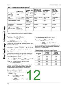
RC5041
PRODUCT SPECIFICATION
• Surround the CEXT timing capacitor with a ground trace
as much as possible. Also be sure to keep a ground or
power plane underneath the capacitor for further noise
isolation. This will help to shield the oscillator pin 1 from
the noise on the PCB. Place this capacitor as close to the
RC5041 pin 1 as possible.
PCB Layout Guidelines and
Considerations
PCB Layout Guidelines
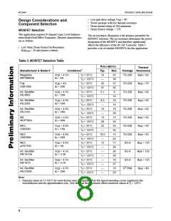
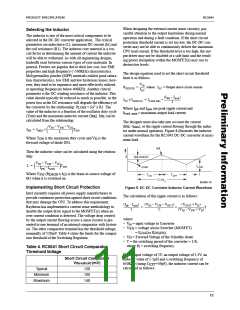
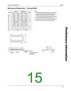
• Placement of the MOSFETs relative to the RC5041 is
critical. The MOSFETs (M1 & M2), should be placed
such that the trace length of the HIDRV pin from the
RC5041 to the FET gates is minimized. A long lead length
on this pin will cause high amounts of ringing due to the
inductance of the trace combined with the large gate
capacitance of the FET. This noise will radiate all over the
board, and because it is switching at such a high voltage
and frequency, it will be very difficult to suppress.
• Place MOSFETs, inductor and Schottky as close together
as possible for the same reasons as #1 above. Place the
input bulk capacitors as close to the drains of MOSFETs
as possible. In addition, placement of a 0.1µF decoupling
cap right on the drain of each MOSFET will help to
suppress some of the high frequency switching noise on
the input of the DC-DC converter.
The drawing below depicts an example of good placement
for the MOSFETs in relation to the RC5041
and also an example of problematic placement for the
MOSFETs.
• The traces that run from the RC5041 IFB (pin 3) and VFB
(pin 4) pins should be run together next to each other and
be Kelvin connected to the sense resistor. Running these
lines together will help in rejecting some of the common
noise that is presented to the RC5041 feedback input. Try
as much as possible to run the noisy switching signals
(HIDRV & VCCQP) on one layer; and use the inner layers
for only power and ground. If the top layer is being used to
route all of the noisy switching signals, use the bottom
layer to route the analog sensing signals VFB and IFB.
In general, all of the noisy switching lines should be kept
away from the quiet analog section of the RC5041. That is
to say, traces that connect to pins 8 and 9 (HIDRV and
VCCQP) should be kept far away from the traces that
connect to pins 1 through 4, and pin 12.
• Place decoupling capacitors (.1µF) as close to the RC5041
pins as possible. Extra lead length on these will negate
their ability to suppress noise.
• Each VCC and GND pin should have its own via down to
the appropriate plane underneath. This will help give
isolation between pins.
M1
M2
Poor layout
Correct layout
9
9
8
7
8
7
10
11
12
13
10
11
12
13
6
6
5
4
5
4
14
15
16
14
15
16
3
2
3
2
1
1
=
“Quiet" Pins
M1
M2
65-5041-12
Figure 10. MOSFET Layout Guidelines
14

 RAYTHEON [ RAYTHEON COMPANY ]