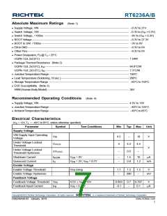
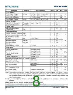
RT6236A/B
Parameter
PVCC Output
Symbol
Test Conditions
Min
Typ
Max
Unit
PVCC Output Voltage
PVCC Line Regulation
PVCC Load Regulation
PVCC Output Current
Internal MOSFET
VPVCC
6V VIN 18V, 0 < IPVCC 5mA
6V VIN 18V, IPVCC = 5mA
0 IPVCC 20mA
--
--
--
--
5
--
--
20
100
--
V
mV
mA
--
IPVCC
VIN = 6V, VPVCC = 4V, TA = 25C
150
RDS(ON)_H
RDS(ON)_L
High-Side On-Resistance
Low-Side On-Resistance
Current Limit
VBOOT VSW = 5V
--
--
51
18
--
--
m
A
Low-Side Switch Valley
Current Limit
ILIM
6.6
7.7
8.9
Thermal Shutdown
Thermal Shutdown Threshold TSD
Thermal Shutdown Hysteresis TSD
On-Time Timer Control
--
--
150
20
--
--
C
On-Time
tON
VOUT = 1.2V
--
--
--
153
60
--
--
--
Minimum On-Time
Minimum Off-Time
Soft-Start
tON_MIN
tOFF_MIN
ns
230
Internal Charge Current
Power Good
VSS = 0V
5
6
7
A
VFB rising (Good)
VFB rising (Fault)
VFB falling (Good)
VFB falling (Fault)
PGOOD = 0.1V
85
--
90
120
112
80
95
--
PGOOD Good Rising
Threshold
%VFB
mA
--
--
PGOOD Good Falling
Threshold
--
--
PGOOD Sink Current
10
20
--
Output Under Voltage and Over Voltage Protections
OVP Trip Threshold
OVP detect
115
--
120
10
125 %VFB
OVP Propagation Delay
--
65
--
s
UVP detect
Hysteresis
55
--
60
UVP Trip Threshold
%VFB
10
UVP Propagation Delay
UVP Enable Delay
--
250
--
s
tSS
x 1.7
Relative to soft-start time
--
--
ms
Note 1. Stresses beyond those listed “Absolute Maximum Ratings” may cause permanent damage to the device. These are
stress ratings only, and functional operation of the device at these or any other conditions beyond those indicated in
the operational sections of the specifications is not implied. Exposure to absolute maximum rating conditions may
affect device reliability.
Note 2. θJA is measured at TA = 25°C on a highly thermal conductive 4-Layer test board. θJC is measured at the top of the
package.
Note 3. Devices are ESD sensitive. Handling precaution is recommended.
Note 4. The device is not guaranteed to function outside its operating conditions.
Copyright 2018 Richtek Technology Corporation. All rights reserved.
©
is a registered trademark of Richtek Technology Corporation.
www.richtek.com
8
DS6236A/B-03 January 2018

 RICHTEK [ RICHTEK TECHNOLOGY CORPORATION ]