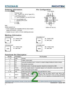
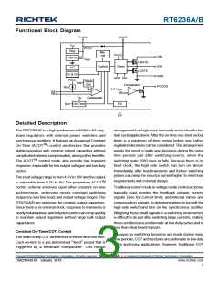
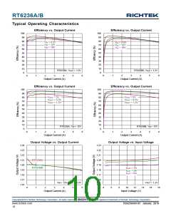
RT6236A/B
Shut-down, Start-Up and Enable (EN)
to its regulated level. After VSS rises above about 2.2V
output over- and under-voltage protections are enabled and
the RT6236A/B begins continuous-switching operation.
The enable input (EN) has a logic-low level of 0.4V. When
VEN is below this level the IC enters shutdown mode and
supply current drops to less than 10μA. When VEN exceeds
its logic-high level of 2V the IC is fully operational.
Internal Regulator (PVCC)
An internal linear regulator (PVCC) produces a 5V supply
from VIN. The 5V power supplies the internal control
circuit, such as internal gate drivers, PWM logic, reference,
analog circuitry, and other blocks. 1μF ceramic capacitor
for decoupling and stability is required.
Between these 2 levels there are 2 thresholds (1.2V typical
and 1.4V typical). When VEN exceeds the lower threshold
the internal bias regulators begin to function and supply
current increases above the shutdown current level.
Switching operation begins when VEN exceeds the upper
threshold. Unlike many competing devices, EN is a high
voltage input that can be safely connected to VIN (up to
18V) for automatic start-up.
PGOOD Comparator
PGOODis an open-drain output controlled by a comparator
connected to the feedback signal. If FB exceeds 90% of
the internal reference voltage or OVP event is cleared,
PGOODwill be high impedance. Otherwise, the PGOOD
output is connected to GND.
Input Under-Voltage Lock-Out
In addition to the enable function, the RT6236A/B feature
an Under-Voltage Lock-Out (UVLO) function that monitors
the internal linear regulator output (VIN). To prevent
operation without fully-enhanced internal MOSFET
switches, this function inhibits switching when VIN drops
below the UVLO-falling threshold. The IC resumes
switching when VIN exceeds the UVLO-rising threshold.
External Bootstrap Capacitor (CBOOT
)
Connect a 0.1μF low ESR ceramic capacitor between
BOOT and SW. This bootstrap capacitor provides the gate
driver supply voltage for the high-sideN-channel MOSFET
switch.
Some of case, such like duty ratio is higher than 65%
application or input voltage is lower than 5.5V which are
recommended to add an external bootstrap diode between
an external 5V and BOOT pin for efficiency improvement
The bootstrap diode can be a low cost one such as IN4148
or BAT54. The external 5V can be a 5V fixed input from
system or a 5V output of the RT6236A/B. Note that the
external boot voltage must be lower than 5.5V
Soft-Start (SS)
The RT6236A/B soft-start uses an external pin (SS) to
clamp the output voltage and allow it to slowly rise. After
VEN is high and VIN exceeds its UVLO threshold, the IC
begins to source 6μAfrom the SS pin.An external capacitor
at SS is used to adjust the soft-start timing. Following
below equation to get the minimum capacitance range in
order to avoid UV occur.
C
V
0.61.2
OUT
OUT
T =
C
Over-Temperature Protection
I
Load Current 0.8
LIM
The RT6236A/B includes an Over-Temperature Protection
(OTP) circuitry to prevent overheating due to excessive
power dissipation. The OTP will shut down switching
operation when the junction temperature exceeds 150°C.
Once the junction temperature cools down by
approximately 20°C the IC will resume normal operation
with a complete soft-start. For continuous operation,
provide adequate cooling so that the junction temperature
does not exceed 150°C.
T6μA
SS
V
REF
Do not leave SS unconnected. During start-up, while the
SS capacitor charges, the RT6236A/B operates in
discontinuous switching mode with very small pulses. This
prevents negative inductor currents and keeps the circuit
from sinking current. Therefore, the output voltage may
be pre-biased to some positive level before start-up. Once
the VSS ramp charges enough to raise the internal reference
above the feedback voltage, switching will begin and the
output voltage will smoothly rise from the pre-biased level
Copyright 2018 Richtek Technology Corporation. All rights reserved.
©
is a registered trademark of Richtek Technology Corporation.
www.richtek.com
6
DS6236A/B-03 January 2018

 RICHTEK [ RICHTEK TECHNOLOGY CORPORATION ]