FDS_6533_6534_004
71M6533/71M6534 Data Sheet
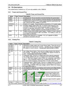
5.9 Pin Descriptions
Pins marked with an asterisk (e.g. V2*) are only available on the 71M6534.
5.9.1 Power and Ground Pins
Table 86: Power and Ground Pins
Name
GNDA
Type Circuit Description
–
–
–
P
P
P
Analog ground: This pin should be connected directly to the ground plane.
Digital ground: This pin should be connected directly to the ground plane.
GNDD
V3P3A
Analog power supply: A 3.3 V power supply should be connected to this
pin, must be the same voltage as V3P3SYS.
–
V3P3SYS
V3P3D
P
System 3.3 V supply. This pin should be connected to a 3.3 V power supply.
O
13
Auxiliary voltage output of the chip. In mission mode, this pin is con-
nected to V3P3SYS by the internal selection switch. In BROWNOUT
mode, it is internally connected to VBAT. V3P3D is floating in LCD and
sleep mode. A bypass capacitor to ground should not exceed 0.1 µF.
VBAT
V2P5
P
12
10
Battery backup and oscillator power supply. A battery or super-capacitor
is to be connected between VBAT and GNDD. If no battery is used, con-
nect VBAT to V3P3SYS.
O
Output of the internal 2.5 V regulator. A 0.1 µF capacitor to GNDA
should be connected to this pin.
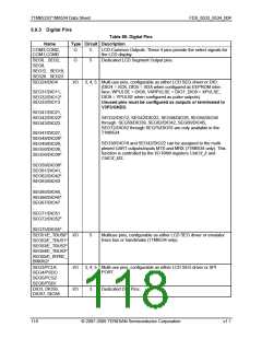
5.9.2 Analog Pins
Table 87: Analog Pins
Name
Type Circuit Description
IAP/IAN,
IBP/IBN,
ICP/ICN
IDP/IDN
I
6
Differential or single-ended Line Current Sense Inputs: These pins are vol-
tage inputs to the internal A/D converter. Typically, they are connected to
the outputs of current sensors. Unused pins must be tied to V3P3A.
VA, VB,
VC
I
I
6
7
Line Voltage Sense Inputs: These pins are voltage inputs to the internal
A/D converter. Typically, they are connected to the outputs of resistor di-
viders. Unused pins must be tied to V3P3A.
V1
Comparator Input: This pin is a voltage input to the internal comparator.
The voltage applied to the pin is compared to the internal BIAS voltage
(1.6 V). If the input voltage is above VBIAS, the comparator output will be
high (1). If the comparator output is low, a voltage fault will occur. A se-
ries 5 kΩ resistor should be connected from V1 to the resistor divider.
V2*
I
7
Comparator Input (71M6534 only): This pin is a voltage input to an internal
comparator. The voltage applied to this pin is compared to an internal ref-
erence voltage (VBIAS). If the input voltage is above VBIAS, the compara-
tor output will be high (1).
VBIAS*
VREF
O
O
9
9
Low-impedance output for use in biasing current sensors and voltage dividers.
Voltage Reference for the ADC. This pin should be left unconnected
(floating).
XIN
XOUT
I
8
Crystal Inputs: A 32 kHz crystal should be connected across these pins.
Typically, a 33 pF capacitor is also connected from XIN to GNDA and a
15 pF capacitor is connected from XOUT to GNDA. It is important to mi-
nimize the capacitance between these pins. See the crystal manufacturer
datasheet for details.
If an external clock is used, a 150 mV (p-p) clock signal should be applied
to XIN, and XOUT should be left unconnected.
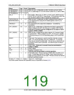
Pin types: P = Power, O = Output, I = Input, I/O = Input/Output
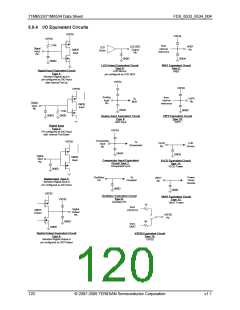
The circuit number denotes the equivalent circuit, as specified under Section 5.9.4 I/O Equivalent Circuits.
v1.1
© 2007-2009 TERIDIAN Semiconductor Corporation
117

 TERIDIAN [ TERIDIAN SEMICONDUCTOR CORPORATION ]