U62H64
Symbol
Unit
Min.
Max.
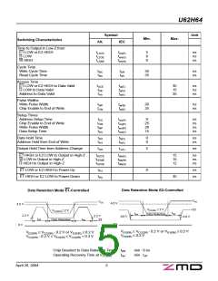
Switching Characteristics
Alt.
IEC
Time to Output in Low-Z from
E1 LOW or E2 HIGH
G LOW
tLZCE
tLZOE
tLZWE
ten(E)
ten(G)
ten(W)
5
0
0
ns
ns
ns
W HIGH
Cycle Time
Write Cycle Time
Read Cycle Time
tWC
tRC
tcW
tcR
35
35
ns
ns
Access Time
E1 LOW or E2 HIGH to Data Valid
G LOW to Data Valid
Address to Data Valid
tACE
tOE
tAA
ta(E)
ta(G)
ta(A)
35
15
35
ns
ns
ns
Pulse Widths
Write Pulse Width
Chip Enable to End of Write
tWP
tCW
tw(W)
tw(E)
20
25
ns
ns
Setup Times
Address Setup Time
Chip Enable to End of Write
Write Pulse Width
Data Setup Time
tAS
tCW
tWP
tDS
tsu(A)
tsu(E)
tsu(W)
tsu(D)
0
ns
ns
ns
ns
25
20
15
Data Hold Time
tDH
tAH
th(D)
th(A)
0
0
ns
ns
Address Hold from End of Write
Output Hold Time from Address Change
tOH
tv(A)
5
ns
E1 HIGH or E2 LOW to Output in High-Z
W LOW to Output in High-Z
tHZCE
tHZWE
tHZOE
tdis(E)
tdis(W)
tdis(G)
15
15
12
ns
ns
ns
G HIGH to Output in High-Z
E1 LOW or E2 HIGH to Power-Up
E1 HIGH or E2 LOW to Power-Down
tPU
tPD
0
ns
ns
35
Data Retention Mode E2-Controlled
Data Retention Mode E1-Controlled
VCC
E2
VCC
4.5 V
0 V
4.5 V
V
CC(DR) ≥ 2 V
V
CC(DR) ≥ 2 V
trec
tDR
Data Retention
2.2 V
2.2 V
E1
0.8 V
0.8 V
tDR
trec
Data Retention
0 V
V
V
E1(DR) ≥ VCC(DR) - 0.2 V or VE1(DR) ≤ 0.2 V
E2(DR) ≤ 0.2 V
V
V
E2(DR) ≥ VCC(DR) - 0.2 V or VE2(DR) ≤ 0.2 V
CC(DR) - 0.2 V ≤ VE1(DR) ≤ VCC(DR) + 0.3 V
Chip Deselect to Data Retention Time
Operating Recovery Time at VCC(DR)
tDR
trec
:
:
min 0 ns
min tcR
April 20, 2004
5

 ZMD [ Zentrum Mikroelektronik Dresden AG ]