INPUT
LATCH
CAP0
0.1 µF
PLL / CLOCK
GENERATOR
INTERNAL
CLOCKS
ED
FF
CAP1
CONTROL
LOGIC
CAV*
DAV*
FLAG
+
C-FIELD
ENCODER
STRBOUT
HCLK
SIGN
LOCKED
DOUT
LOUT
D0-D19
RST*
D-FIELD
ENCODER
FRAME
MUX
OUTPUT
SELECT
INV
LOOPEN
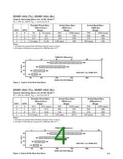
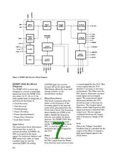
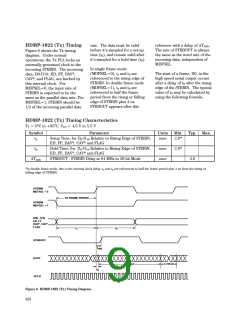
Figure 4. HDMP-1022 Transmitter Block Diagram.
HDMP-1022 Tx Block
Diagram
STRBIN is expected to be the
incoming frame clock. The PLL/
Clock Generator locks on to this
incoming rate and multiplies the
clock up to the needed high speed
serial clock. Based on M20SEL,
which determines whether the
incoming data frame is 16 or 20
bits wide, the PLL/Clock Gener-
ator multiplies the frame rate
clock by 20 or 24 respectively
(data bits + 4 control bits). DIV1/
DIV0 are set to inform the
transmitter of the frequency range
of the incoming data frames. The
internal frame rate clock is
accessible through STRBOUT and
the high speed serial clock is
accessible through HCLK.
the transmitter. The clock
generator section performs the
clock multiplication to the
necessary serial clock rate.
The HDMP-1022 was designed to
accept 16 or 20 bit wide parallel
data (frames) and transmit it over
a high speed serial line, while
minimizing the user’s necessary
interface to the high speed cir-
cuitry. In order to accomplish this
task, the HDMP-1022 performs
the following functions:
By setting EHCLKSEL high, the
user may provide an external high
speed serial clock at STRBIN.
This clock is used directly by the
high speed serial circuitry to
output the serial data.
• Parallel Word Input
• High Speed Clock Multiplication
• Frame Encoding
Control Logic and C-Field
Encoder
The Control Logic is responsible
for determining what information
is serially sent to the output. If
CAV* is low, it sends the data at
D0..D8 and D9..D17 as control
word information. If CAV* is high
and DAV* is low, it sends parallel
word data at the data inputs. If
neither CAV* nor DAV* is set low,
then the transmitter assumes the
link is not being used. In this
state, the control logic triggers
the Data Encoder to send Fill
Frames to maintain the link DC
• Parallel to Serial Multiplexing
PLL/Clock Generator
The Phase Lock-loop and Clock
Generator are responsible for
generating all internal clocks
needed by the transmitter to
perform its functions. These
clocks are based on a supplied
frame clock (STRBIN) and control
signals (M20SEL, MDFSEL,
EHCLKSEL, DIV1, DIV0). In
normal operation (MDFSEL=0),
When MDFSEL is set high, the
transmitter is in Double Frame
Mode. Using this option, the user
may send a 32 or 40 bit wide data
frame in two segments while
supplying the original 32 or 40 bit
frame clock at STRBIN. Doubling
of the frame rate is performed by
620

 AGILENT [ AGILENT TECHNOLOGIES, LTD. ]