AO4459
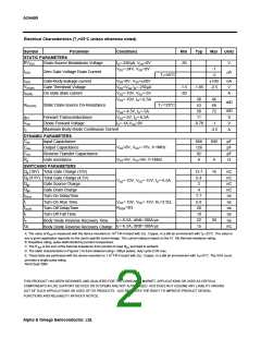
Electrical Characteristics (TJ=25°C unless otherwise noted)
Symbol
Parameter
Conditions
Min
Typ
Max
Units
STATIC PARAMETERS
BVDSS
Drain-Source Breakdown Voltage
ID=-250µA, VGS=0V
-30
V
VDS=-24V, VGS=0V
-1
-5
IDSS
Zero Gate Voltage Drain Current
µA
TJ=55°C
IGSS
Gate-Body leakage current
Gate Threshold Voltage
On state drain current
V
V
V
V
DS=0V, VGS=±20V
DS=VGS ID=-250µA
GS=-10V, VDS=-5V
GS=-10V, ID=-6.5A
±100
-2.5
nA
V
VGS(th)
ID(ON)
-1.5
-30
-1.85
A
38
53
46
68
72
mΩ
mΩ
RDS(ON)
TJ=125°C
Static Drain-Source On-Resistance
VGS=-4.5V, ID=-5A
58
gFS
VSD
IS
Forward Transconductance
Diode Forward Voltage
VDS=-5V, ID=-6.5A
IS=-1A,VGS=0V
11
S
V
A
-0.78
-1
Maximum Body-Diode Continuous Current
-3.5
DYNAMIC PARAMETERS
Ciss
Coss
Crss
Rg
Input Capacitance
668
126
92
830
pF
pF
pF
Ω
V
GS=0V, VDS=-15V, f=1MHz
Output Capacitance
Reverse Transfer Capacitance
Gate resistance
V
GS=0V, VDS=0V, f=1MHz
6
9
SWITCHING PARAMETERS
Qg (10V)
Total Gate Charge (10V)
Total Gate Charge (4.5V)
Gate Source Charge
Gate Drain Charge
12.7
6.4
2
16
nC
nC
nC
nC
ns
Qg (4.5V)
V
GS=-10V, VDS=-15V, ID=-6.5A
Qgs
Qgd
tD(on)
tr
4
Turn-On DelayTime
Turn-On Rise Time
Turn-Off DelayTime
Turn-Off Fall Time
7.7
6.8
20
10
22
15
VGS=-10V, VDS=-15V, RL=2.5Ω,
ns
RGEN=3Ω
tD(off)
tf
ns
ns
trr
IF=-6.5A, dI/dt=100A/µs
IF=-6.5A, dI/dt=100A/µs
30
Body Diode Reverse Recovery Time
Body Diode Reverse Recovery Charge
ns
nC
Qrr
A: The value of RθJA is measured with the device mounted on 1in2 FR-4 board with 2oz. Copper, in a still air environment with TA =25°C. The value in
any a given application depends on the user's specific board design. The current rating is based on the t≤ 10s thermal resistance rating.
B: Repetitive rating, pulse width limited by junction temperature.
C. The RθJA is the sum of the thermal impedence from junction to lead RθJL and lead to ambient.
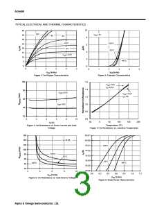
D. The static characteristics in Figures 1 to 6are obtained using< 300µs pulses, duty cycle 0.5% max.
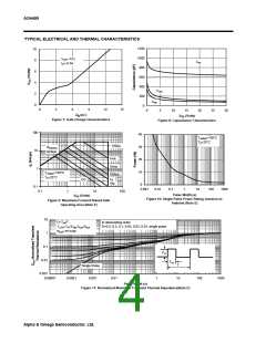
E. These tests are performed with the device mounted on 1 in2 FR-4 board with 2oz. Copper, in a still air environment with TA=25°C. The SOA curve
provides a single pulse rating.
Rev0 Sept 2006
THIS PRODUCT HAS BEEN DESIGNED AND QUALIFIED FOR THE CONSUMER MARKET. APPLICATIONS OR USES AS CRITICAL
COMPONENTS IN LIFE SUPPORT DEVICES OR SYSTEMS ARE NOT AUTHORIZED. AOS DOES NOT ASSUME ANY LIABILITY ARISING
OUT OF SUCH APPLICATIONS OR USES OF ITS PRODUCTS. AOS RESERVES THE RIGHT TO IMPROVE PRODUCT DESIGN,
FUNCTIONS AND RELIABILITY WITHOUT NOTICE.
Alpha & Omega Semiconductor, Ltd.

 AOS [ ALPHA & OMEGA SEMICONDUCTORS ]